At a Glance
For five decades, the semiconductor industry optimized a single variable: transistor density on a monolithic die. That variable is no longer enough. A confluence of physical limits — the reticle boundary, non-linear yield degradation, and the uneven economics of process node advancement — has made the monolithic system-on-chip (SoC) structurally inadequate for the most demanding applications in compute.
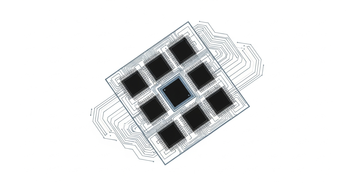
The chiplet paradigm is the industry's answer. Rather than integrating every function onto one continuous piece of silicon, chiplet-based designs disaggregate the SoC into multiple independently manufactured dies, each optimized for its function, assembled into a single package. The promise is real: higher yields, lower cost per function, and the ability to mix process nodes — running high-speed logic on TSMC N3 while keeping analog I/O on a stable 28nm node that has been characterized for decades.
But disaggregation creates a new problem. If a monolithic chip's internal buses are replaced by die-to-die interconnects between separately manufactured dies — potentially from different vendors — those interconnects must be fast enough to be transparent to the system, efficient enough not to erode the gains from heterogeneous integration, and standardized enough to allow a multi-vendor ecosystem to exist at all.
The Universal Chiplet Interconnect Express (UCIe) standard, announced in March 2022 by a founding consortium that includes Intel, TSMC, Samsung, Qualcomm, AMD, Arm, Meta, Microsoft, Google, and ASML, is the industry's attempt to supply that standardization. Understanding what UCIe actually decides — and what it deliberately leaves unsolved — requires working through its design from the physical layer up.
That's what this article does.
The Load-Bearing Constraint: Bandwidth Density vs. Energy Per Bit
Every design decision in UCIe traces back to a single, unforgiving tradeoff: bandwidth density versus energy per bit.

Bandwidth density — measured in gigabits per second per millimeter of interconnect width, or terabits per second per square millimeter for area-constrained interposer links — determines how much data can cross the die boundary in a given silicon footprint. Energy per bit, measured in picojoules per bit, determines what that data movement costs in power. These two variables pull in opposite directions. Maximizing bandwidth density generally requires tighter bump pitches, shorter signal paths, and higher signaling frequencies — all of which increase the energy required per transmitted bit and impose tighter process tolerances.
The following table, drawn from the research literature, frames the landscape:
| Interconnect Technology | Bandwidth Density | Energy per Bit | Representative Use |
|---|---|---|---|
| PCIe 5.0 (off-package) | ~1 Gb/s/mm | ~10–15 pJ/bit | GPU to CPU |
| TSMC CoWoS (Si Interposer) | >1 Tb/s/mm² | ~0.5–1 pJ/bit | HBM to GPU |
| Intel EMIB | ~1 Tb/s/mm² | ~0.5 pJ/bit | Foveros stacks |
| UCIe (on-package, advanced) | Up to 28 Gb/s/pin | ~0.5 pJ/bit | Multi-vendor chiplets |
The gap between PCIe 5.0 and on-package interconnects isn't incremental — it's an order of magnitude in energy efficiency and multiple orders of magnitude in bandwidth density. Moving a function from an off-package PCIe link to an on-package UCIe link isn't an optimization of the same architecture. It's a category change in what the system can do.
This table is the load-bearing constraint that determines every UCIe design decision above it. When the specification chooses a forwarded-clock architecture, defines two distinct PHY variants, or specifies a flit-based flow control unit, those choices are engineering responses to the physical reality encoded in this tradeoff. Understanding UCIe means understanding why each layer answers the question the layer below it creates.
Why the Physics Forces the Architecture: Three Converging Limits
Before descending into the UCIe stack, it's worth establishing — precisely, not rhetorically — why the chiplet transition is structural rather than cyclical.
The Reticle Wall
A modern EUV lithography stepper exposes a maximum area of approximately 858 mm² per shot. A monolithic die can't exceed this area; anything larger requires stitching multiple reticle shots together, which introduces alignment errors that degrade yield at the stitch boundaries. As leading-edge designs push toward this boundary, chiplets become the only viable path to greater transistor counts within a single package.
This isn't a limitation that will be engineered away. It's a consequence of optical diffraction physics. The reticle limit doesn't move; the die must.
The Yield Curve
Yield on a silicon wafer isn't a linear function of die area. Defect density follows a Poisson statistical distribution: given a fixed number of defects per unit area, larger dies encounter proportionally more defects, and the probability that any single defect falls within a given die's critical area increases non-linearly with that area.
The consequence, formalized in the academic literature since at least 2017, is that a large monolithic die may yield at 30–40% on a leading-edge process — meaning six out of every ten dies fabricated are non-functional. Two smaller dies, each covering roughly half the area, might yield at 70–80% each. The total number of functional die-pairs per wafer substantially exceeds the number of functional monolithic dies, even after accounting for assembly cost.
This is the quantitative foundation of the chiplet business case. Not a marketing argument about flexibility or ecosystem optionality. A straightforward cost calculation driven by semiconductor physics.
Process Node Heterogeneity
The third driver is less intuitive but equally fundamental. The semiconductor industry's narrative around process nodes — smaller is better, N3 beats N5 beats N7 — holds for digital logic operating in a narrow frequency and voltage range. It doesn't hold for the full range of functions a modern SoC integrates.
Analog circuits, SerDes transceivers, and high-voltage I/O are deliberately designed on mature nodes — 28nm, 65nm, sometimes older. The reason isn't cost alone. On leading-edge nodes at 5nm or 3nm, transistor threshold voltages become so low that analog circuits struggle with noise margins, leakage currents disrupt precision analog behavior, and the thin gate oxides that enable digital performance create reliability problems for circuits operating at elevated voltages. A 28nm SerDes built on a well-characterized mature node isn't a compromise. It's frequently a better SerDes — at lower cost, with higher reliability — than one forced onto N3 to share a monolithic die with the compute cores.
Chiplet architecture unlocks this insight structurally. Once the SoC is disaggregated, each function can be assigned to its optimal process node. The compute tiles run at the frontier; the analog I/O runs where analog performs best. This principle — heterogeneous integration — is the architectural payoff that yield economics alone doesn't fully capture.
Together, these three forces make chiplets not merely viable but, for the most demanding designs, unavoidable. The question isn't whether the industry will adopt a chiplet model. It's what the interconnect standard that makes multi-vendor chiplet composition possible will look like.
UCIe: A Layered Protocol Stack, Not a Wire Standard
The most consequential framing error in mainstream UCIe coverage is treating it as an interconnect — a faster, shorter wire between dies. UCIe isn't a wire standard. It's a four-layer protocol stack, and its architecture mirrors a network stack with deliberate precision. Understanding the design rationale at each layer is the difference between knowing what UCIe specifies and understanding why it was designed that way.

Layer 1: The Physical Layer — Two PHYs for Two Realities
UCIe's physical layer defines two distinct variants — not as a compromise, but as a principled acknowledgment that the chiplet packaging market spans two cost-performance regimes with fundamentally different constraints.
The Standard Package PHY targets organic substrates — the laminate packages that dominate high-volume consumer and server silicon. Organic substrates are cheaper and available at scale from a mature supply chain. Their limitation is dimensional tolerance: the polymer materials in organic laminates expand and contract with temperature at rates that differ from silicon, and the minimum bump pitch achievable without unacceptable failure rates is constrained. The Standard Package PHY targets bump pitches of 100 µm and above, operating at up to 16 Gb/s per lane. These are numbers that work with existing organic substrate manufacturing infrastructure.
The Advanced Package PHY targets silicon interposers (as in TSMC's CoWoS) and embedded silicon bridges (as in Intel's EMIB). Both approaches use silicon — rather than polymer — as the routing medium between dies, enabling significantly tighter dimensional tolerances. The Advanced Package PHY targets bump pitches down to 25 µm and operates at up to 32 Gb/s per lane — double the speed of the standard variant, at a fraction of the bump pitch.
Both variants use a source-synchronous forwarded clock architecture. In source-synchronous design, the transmitter sends a clock signal alongside the data, phase-aligned to the data at the source. The receiver uses this forwarded clock to sample the data, rather than deriving timing from a local reference. At the data rates UCIe targets — 16 to 32 Gb/s per lane — source-synchronous clocking is a practical necessity: the clock-to-data skew introduced by independently generated clocks at each die would be comparable to the bit period itself, making reliable sampling impossible without forwarded clock alignment.
This is the layer that determines cost, density, and raw bandwidth. Every design decision above it is constrained by what the PHY can deliver. The Advanced Package PHY's 32 Gb/s per lane is the ceiling that protocol designers at Layer 2 and above must work within.
Layer 2: The Die-to-Die Adapter — The Reliability Envelope
If the physical layer is the foundation, the D2D adapter is the structure. It transforms a physical signaling link into something a system can depend on — and it's the layer most conspicuously absent from mainstream UCIe coverage.
The D2D adapter handles four distinct functions:
Flow Control. UCIe uses a flit (Flow Control Unit) structure for organizing data transmission. A flit is the atomic unit of transfer at the link layer — analogous to a packet at the network layer, but defined by the physical link's flow control state rather than by routing considerations. Flit-based flow control allows the receiver to signal back to the transmitter when its buffers are approaching capacity, throttling the data stream before overflow occurs. This isn't a trivial mechanism at 32 Gb/s per lane — the round-trip latency for a flow control signal across a die-to-die link is short enough to be useful, which is precisely why in-package links enable flit-based flow control where off-package links cannot.
Link Training. When a UCIe link initializes, the two endpoints must negotiate their operating parameters — lane count, speed, equalization settings, and clock alignment. Link training is the handshake protocol that brings a UCIe link from powered-up silence to reliable high-speed operation. The complexity of link training increases with speed: at 32 Gb/s per lane, the equalization required to compensate for channel loss and crosstalk on even a short silicon interposer path is non-trivial, and the training sequence must converge quickly enough to meet system bring-up time requirements.
Power Management. UCIe defines power states for the die-to-die link — active, low-power standby, and off — with transition protocols that allow the link to scale power consumption with traffic load. In AI inference workloads, where a chiplet may sit idle between inference requests, power state management is a first-order concern. The D2D adapter enforces the link's power state machine, independent of what protocols are running above it.
Error Correction. At the D2D adapter layer, UCIe implements link-level error detection and, in certain configurations, correction. This is the mechanism that makes UCIe suitable for applications where data integrity is non-negotiable — including, potentially, automotive safety-critical functions (a topic we return to in the speculation section below). Without link-level error handling at Layer 2, every protocol running above UCIe would need to implement its own error recovery, fragmenting the ecosystem and imposing redundant overhead.
The D2D adapter answers a different question than the PHY does. The PHY answers the bandwidth question. The D2D adapter answers the dependability question. For any deployment beyond consumer electronics — servers, automotive ADAS, telecommunications infrastructure — the D2D adapter's capabilities are the determining factor.
Layer 3: The Protocol Stack — The Strategic Crux
Layer 3 is where UCIe's most consequential design decision lives. It's also the decision that determines whether UCIe becomes infrastructure or a footnote.
UCIe's protocol layer is deliberately protocol-agnostic. The same UCIe link can carry:
- PCIe (TLP-level semantics) — the transaction layer protocol governing the industry-standard peripheral interconnect, enabling UCIe to function as an in-package PCIe fabric
- CXL (Compute Express Link) — including CXL.io for device attachment, CXL.cache for host-to-device cache coherency, and CXL.mem for memory pooling and disaggregation
- AXI streaming protocols — the AMBA-based fabric widely used in AI accelerator internal datapaths
- Vendor-proprietary protocols — preserving the ability for vendors to use UCIe's physical and link layers while running custom protocols above them
This protocol agnosticism isn't a feature list item. It's the structural decision that determines UCIe's long-term relevance.
Consider what CXL-over-UCIe implies concretely. CXL's most technically interesting capability — CXL.mem — enables a host processor to address memory attached to a device across the CXL link as if it were local DRAM, with cache-coherent semantics. At board level, a CXL.mem link traverses a PCIe slot and a PCIe switch, accumulating latency measured in hundreds of nanoseconds. The memory coherency benefits are real, but the latency overhead limits the use cases.
When CXL.mem runs over a UCIe link within the same package, the latency collapses by orders of magnitude. The cache-coherent memory pooling that CXL promises becomes practical across a heterogeneous chiplet ensemble: a compute die and a memory-controller die from different vendors, assembled on a common interposer, communicating via a UCIe link carrying CXL.mem, with sub-ten-nanosecond latency for cache-coherent memory access. This isn't a marginal improvement over current AI accelerator memory architectures. It's a different architecture — one that could eventually allow AI systems to pool and dynamically allocate memory across chiplet boundaries without the fixed-topology constraints of today's HBM stacking.
The protocol agnosticism also defines the failure mode. If UCIe's protocol layer becomes balkanized — if each major vendor runs its own proprietary protocol above the UCIe PHY and D2D adapter — then UCIe becomes a physical transport layer that enables multi-vendor assembly without enabling multi-vendor interoperability at the system level. The result would be cheaper packaging, not an open ecosystem. The industry's experience with prior interconnect standardization efforts, including early PCIe and USB implementations where vendor-specific extensions fragmented interoperability, provides a precedent the UCIe Consortium is clearly aware of.
The degree to which Layer 3 remains genuinely open — and the degree to which the compliance program enforces interoperability across vendors running the same protocol — will determine UCIe's ultimate strategic significance.
Layer 4: The Sideband Channel — The Overlooked Infrastructure Layer
UCIe's sideband channel is perhaps the least-discussed element of the specification. It's arguably the most important for anyone deploying UCIe-based systems in real infrastructure.
The sideband channel is a low-speed communication path, separate from the main data path, reserved for configuration, debug, and management traffic. Its significance is clearest in the context of what it enables at the firmware level.
In a monolithic SoC, the chip presents a single, unified identity to the system firmware. UEFI initializes one die; the operating system sees one device. In a UCIe-based multi-chiplet package, the system firmware must be aware that multiple dies — potentially from different vendors, manufactured on different processes, with different power domains and reliability characteristics — are assembled into what presents as a single package. The sideband channel provides the communication infrastructure for chiplet enumeration: the process by which system firmware or a hypervisor discovers, identifies, and configures the individual chiplets within an assembled package.
This has non-trivial implications for datacenter infrastructure. A hypervisor managing a multi-tenant workload on a chiplet-based AI accelerator needs visibility into individual chiplet health, power consumption, and error rates to make intelligent scheduling decisions. The sideband channel is the mechanism through which that visibility is delivered. Without it, the package is a black box; with it, the package becomes a managed ensemble of discrete, observable components.
The firmware and software ecosystem that will ultimately leverage UCIe's sideband channel — UEFI extensions, hypervisor chiplet enumeration drivers, management plane integrations — isn't yet built. The hardware foundation exists in the specification. The software layer above it is the next frontier.
The BUNCH Problem: Why This Standardization Is Harder Than PCIe
UCIe's designers are operating against a historical backdrop of interconnect standardization efforts that didn't generalize as promised. Understanding why chiplet standardization is structurally harder than PCIe or USB standardization is essential context for evaluating UCIe's prospects.

The core challenge can be framed as the BUNCH problem — five distinct dimensions of variance that UCIe must absorb across a multi-vendor ecosystem:
Bandwidth heterogeneity. Different application domains want different bandwidth-to-latency tradeoffs from the die-to-die interface. A high-performance AI training accelerator wants maximum bisection bandwidth across as many UCIe lanes as physically fit on the package perimeter; an automotive edge inference SoC wants minimum energy per bit across a small number of lanes at moderate speed. UCIe's two-PHY approach is a partial answer to this, but the tradeoff space is continuous while the specification offers two discrete points.
Packaging process uncertainty. Advanced packaging processes — silicon interposer fabrication, embedded bridge embedding, hybrid bonding — aren't as mature or as uniformly characterized across foundries as the planar transistor processes that produce the chiplets themselves. Bump height variation across a large interposer, substrate warpage under thermal cycling, and thermal expansion mismatch between silicon dies and organic substrates all introduce signal integrity variability that the UCIe PHY's equalization and training procedures must absorb. The specification defines what the PHY must handle; it doesn't eliminate the underlying process variance.
Noise coupling. When multiple chiplets share the same interposer — a digital compute die operating at multi-GHz clock frequencies, a SerDes die switching at tens of gigabits per second, and an analog signal processing die requiring sub-millivolt noise floors — the substrate itself becomes a noise coupling medium. High-speed digital switching injects substrate currents that appear as noise at the analog die's sensitive nodes. This crosstalk problem is manageable within a single-vendor design where the full substrate is co-designed; it becomes significantly harder when the chiplets come from different vendors with different power delivery architectures and switching profiles.
Cost overhead from compliance. UCIe compliance isn't free in silicon area. Implementing the UCIe PHY and D2D adapter on each participating chiplet requires die area — estimated, pending formal characterization in the literature, at roughly 5–10% of die area per interface. For a chiplet vendor selling into a cost-sensitive market, this overhead is a real barrier to UCIe adoption relative to a proprietary die-to-die interface optimized for a specific product family.
Heterogeneous reliability targets. A DRAM memory chiplet, a high-performance compute chiplet, and an automotive-grade sensor fusion chiplet have different reliability requirements, different temperature operating ranges, and different qualification standards. A UCIe package that assembles all three must satisfy the most demanding reliability requirement of any component — and demonstrating that the assembly satisfies that requirement requires test and qualification procedures that aren't yet standardized across the chiplet supply chain.
These five dimensions explain why UCIe standardization isn't simply a matter of publishing a specification and waiting for adoption. PCIe standardization was challenging, but PCIe standardized an interface between a relatively small number of component categories — host processors, discrete adapters, storage controllers — with relatively uniform electrical environments: a motherboard, a single power domain, a controlled thermal environment. UCIe must standardize an interface that will be used between dozens of chiplet categories, across multiple assembly technologies, in environments ranging from a liquid-cooled datacenter to an automotive underhood module operating at sustained elevated temperature.
The BUNCH problem isn't an argument against UCIe. It's the technical explanation for why the chiplet ecosystem will develop more slowly than the consumer technology press's enthusiasm suggests — and why the Consortium's compliance program, not the specification itself, will be the rate-limiting factor in multi-vendor UCIe adoption.
The Standards Landscape: UCIe's Competitive and Collaborative Context
UCIe doesn't operate in isolation. Its practical deployment occurs within a dense ecosystem of complementary and competing standards.
On the open standards side, UCIe's natural protocol companions are well-defined:
CXL 3.1 is the cache-coherent memory fabric protocol that UCIe was, in large part, designed to carry in-package. CXL and UCIe aren't competing standards; they're complementary layers of a stack — UCIe provides the physical and link infrastructure, CXL provides the coherency semantics above it.
PCIe 6.0 is UCIe's genealogical ancestor and its primary protocol payload for non-coherent device attachment. The transactional semantics of PCIe run natively over UCIe without modification, which means any device driver, operating system PCIe stack, or management plane software designed for board-level PCIe operates transparently over in-package UCIe links.
JEDEC HBM3E defines the interface between high-bandwidth memory stacks and their host dies. HBM3E isn't a competitor to UCIe; HBM's interface is specifically engineered for the extremely high-bandwidth, extremely short-distance connection between a memory stack and the logic die directly beneath it — a configuration where UCIe's overhead wouldn't be appropriate. The two standards address different points in the memory hierarchy.
The proprietary interconnect landscape presents a more complex picture. AMD's Infinity Fabric, IBM's POWER D-Bus, and Intel's internal die-to-die interfaces in Foveros implementations are all proprietary — optimized for their respective product families and not interoperable with chiplets from other vendors. AMD has publicly committed to UCIe adoption in future roadmap products, and Intel's foundational contributions to the UCIe specification mean its physical packaging infrastructure (EMIB, Foveros) is designed to be UCIe-compatible.
The strategically notable absence is NVIDIA. NVIDIA's NVLink 4.0 — the high-bandwidth interconnect used in its H100 and GB200 series accelerators — remains proprietary and is not part of the UCIe Consortium's founding membership roster. NVLink's performance envelope exceeds what UCIe's current specification offers for GPU-scale bandwidth requirements, and NVIDIA's vertical integration across silicon, packaging, software, and systems gives the company less incentive to participate in a standardization effort that would, by design, reduce the moat around its interconnect technology.
This absence has architectural consequences. The most computationally intensive AI workloads today run on NVIDIA silicon, using NVLink for scale-up communication and NVSwitch for multi-GPU fabric. If UCIe's ecosystem matures while NVIDIA maintains a proprietary interconnect wall, the chiplet marketplace's most compelling use case — composable AI accelerators assembled from best-of-breed components — will exist alongside rather than within the dominant AI compute platform.
Whether that parallel existence eventually pressures NVIDIA toward UCIe participation, or whether the NVLink ecosystem becomes self-reinforcing as the AI workload grows, is one of the most consequential open questions in the near-term semiconductor landscape.
Real-World Implementations: Where the Principles Meet Production
The theoretical case for chiplets and the technical architecture of UCIe are validated — and stress-tested — by production implementations. Three deployments are particularly instructive.
Intel Meteor Lake: The Consumer Chiplet Pioneer
Intel's Meteor Lake, released in December 2023, is the first mass-market consumer processor built on a chiplet architecture with die-to-die interconnects consistent with UCIe's principles. The design disaggregates what had previously been a monolithic SoC into four distinct tiles: a compute tile (on Intel's 4nm-class process), an SoC tile (on TSMC N6), a GPU tile (on TSMC N5), and an I/O tile (on TSMC N6). These tiles are assembled using Intel's Foveros Direct hybrid bonding technology.
Meteor Lake's significance isn't performance — the initial generation's performance-per-watt was received with mixed reviews. Its significance is demonstration. Intel assembled a shipping product with silicon from multiple fabs, on multiple process nodes, integrated through an advanced packaging approach that reflects the same physical principles UCIe is designed to standardize. The die-to-die interconnect in Meteor Lake is Intel's internal Foveros implementation, not UCIe v1.1 as specified — but Intel contributed foundational IP to the UCIe specification, and the architectural lineage is direct.
AMD EPYC Genoa: Scale Validation at Production Volume
AMD's EPYC Genoa, based on the Zen 4 core architecture, assembles up to 12 compute chiplets (Core Complex Dies, CCDs) on an I/O die using AMD's proprietary Infinity Fabric. The Infinity Fabric interconnect isn't UCIe-compliant, but EPYC Genoa demonstrates the yield and scalability arguments for chiplets at a scale that validates the economics.
Each Zen 4 CCD is manufactured at TSMC N5, a leading-edge process where a larger monolithic die would suffer significant yield loss. By limiting each CCD to a bounded area and connecting multiple CCDs to a centralized I/O die on a more mature process node, AMD achieves aggregate transistor counts and core densities that a monolithic approach couldn't produce at competitive yields. The I/O die — handling memory controllers, PCIe, and Infinity Fabric routing — runs on a less advanced node where the mixed-signal and high-voltage circuitry it contains is more naturally suited. EPYC Genoa is a commercial-scale proof of heterogeneous integration's economic logic.
Intel Ponte Vecchio: The Stress Test
Ponte Vecchio, Intel's Xe-HPC GPU designed for the Aurora exascale supercomputer, is the most aggressive chiplet implementation yet shipped. It integrates 47 active tiles across five distinct process nodes — Intel 7, TSMC N5, TSMC N7, TSMC N12, and Intel 10 — using both EMIB and Foveros 3D stacking.
Ponte Vecchio is instructive not only as a demonstration of what heterogeneous integration can achieve, but as a stress test that reveals where the principles break down in practice. A 47-tile assembly across five process nodes represents an extreme version of the BUNCH problem: five different process characterizations, five different thermal expansion profiles, five different power delivery requirements, all assembled into a coherent system that must meet a unified reliability specification. The development challenges Ponte Vecchio encountered — schedule delays, yield challenges in the assembly process, and thermal management complexity — are documented in the public record. They're not a reflection of design failure so much as an honest accounting of what the frontier of heterogeneous integration currently costs.
UCIe is, in part, designed to generalize the principles demonstrated by Ponte Vecchio's internal die-to-die architecture across a multi-vendor ecosystem. Ponte Vecchio's experience is therefore the most honest available data point on the gap between what UCIe promises in specification and what multi-die assembly delivers in production. Closing that gap is the engineering challenge that the next five years of chiplet development will be defined by.
The Patent Architecture: Who Owns the Foundational IP
The chiplet and die-to-die interconnect patent landscape is one of the most active in the semiconductor IP domain, and its structure matters for understanding the competitive dynamics of the emerging UCIe ecosystem.
Intel holds foundational packaging IP across two critical families. The Embedded Multi-die Interconnect Bridge (EMIB) family covers the use of a small silicon bridge embedded in an organic substrate to provide high-density die-to-die connectivity without a full silicon interposer — a cost-reducing alternative to TSMC's CoWoS that expands the addressable market for advanced packaging by bringing it within reach of organic substrate assembly. The Foveros 3D stacking family covers face-to-face die stacking using Through-Silicon Vias and micro-bumps, enabling vertical integration with the highest possible bandwidth density and lowest possible latency.
TSMC's CoWoS IP covers the dominant silicon interposer approach for HBM-plus-GPU integration, which underlies NVIDIA's H100, AMD's MI300X, and virtually every other high-end AI accelerator currently in production. CoWoS is the packaging technology that makes today's AI compute infrastructure possible. TSMC's IP position here is a structural advantage that will persist as long as silicon interposers remain the substrate of choice for maximum-bandwidth-density applications.
AMD's chiplet system-level patents cover die-to-die protocol translation and coherency management across disaggregated dies — the system architecture layer above the physical packaging. This IP is directly relevant to UCIe's Layer 3 protocol agnosticism: AMD's published chiplet architecture patents demonstrate that the cache-coherency challenges UCIe's CXL-over-UCIe capability aims to address have been actively researched and filed upon by the major consortium members.
A second wave of patent activity is emerging around UCIe-specific implementations: retimer architectures for extending UCIe link reach, flit encoding schemes optimized for different traffic patterns, power state machine implementations, and debug interface designs for assembled multi-die packages. This second-order IP landscape — covering not the foundational packaging technologies but the specific engineering decisions required to build UCIe-compliant products — will determine which companies capture value in the UCIe supply chain beyond the foundational silicon and packaging IP held by the large incumbents.
For chiplet startups designing specialized AI, RF, or analog chiplets intended to plug into UCIe-based systems, navigating this IP landscape is a critical business consideration. The foundational packaging IP is largely owned by the companies that also control the manufacturing — Intel, TSMC, Samsung. The UCIe protocol IP is being defined collaboratively through the consortium process, with individual members filing around the edges. The white space for independent chiplet developers is real, but it isn't unlimited.
Speculation: The Trajectories That Will Determine UCIe's Significance
The following section is explicitly speculative. It is grounded in the technical trajectories and research directions documented in the academic and industry literature, but it extrapolates beyond confirmed deployments.
The In-Package Memory Fabric
The most technically consequential near-term development in the UCIe ecosystem is the convergence of UCIe as the physical and link layer with CXL as the protocol layer for in-package memory pooling.
Today's AI accelerator memory architecture is determined by a constraint: HBM stacks must be physically proximate to the GPU die they serve, placed on the same silicon interposer, with the interposer acting as the ultra-high-bandwidth memory bus. This is a fixed, vendor-specific topology. The HBM stacks on an H100 serve that H100 and no other device.
A UCIe-plus-CXL.mem architecture opens the possibility of disaggregated memory chiplets — separately manufactured memory controller and buffer chiplets connected to compute dies via UCIe links, with CXL.mem providing cache-coherent addressing across the assembled pool. This would enable a memory topology configured at assembly time rather than determined at design time — more SRAM for latency-sensitive inference, more HBM3E for bandwidth-hungry training, more LPDDR5X for power-constrained edge deployment, all within a single package architecture whose memory composition is determined by which chiplets are assembled onto the interposer.
The technical barriers are real: CXL.mem's coherency protocol adds latency relative to native HBM access, and the packaging density required to achieve comparable bandwidth per watt to integrated HBM stacking through UCIe links isn't yet demonstrated at production scale. But the trajectory is clear, and the research literature on processing-in-memory and disaggregated memory architectures establishes the direction of travel.
The Open Hardware Inflection: RISC-V Chiplets
A development that has received insufficient attention in mainstream coverage is the convergence of the RISC-V open instruction set architecture with the chiplet paradigm.
Open-source RISC-V cores — including the CVA6 out-of-order core from ETH Zurich and the SonicBOOM core from UC Berkeley — are being explored in chiplet contexts: as self-contained, reusable compute chiplets that can be integrated into heterogeneous packages alongside specialized accelerators, I/O chiplets, and memory interfaces. The RISC-V ISA's open licensing removes the per-unit royalty barrier that applies to Arm cores, making RISC-V chiplets economically viable for a range of applications where total system cost is sensitive to IP licensing overhead.
If UCIe and open-source RISC-V chiplets mature on parallel timelines, the result could be a path to a fully composable, open-licensed, multi-vendor System-in-Package — a development with significant implications for sovereign semiconductor programs and for companies seeking to reduce dependency on proprietary ISA licensing for embedded and edge computing applications. The geopolitical dimension of semiconductor supply chain fragmentation, accelerated by export control regimes that constrain access to advanced chips across national boundaries, makes this trajectory more than an academic curiosity.
The Automotive Gap
UCIe's standard package PHY, with its organic substrate targeting and 100 µm or greater bump pitch, has a natural application path to automotive SoCs — the domain of ADAS processing, sensor fusion, and autonomous driving compute. The cost and volume economics of organic substrate assembly align well with automotive manufacturing requirements.
The gap is functional safety. Automotive electronics deployed in safety-critical roles must meet ISO 26262 ASIL-D requirements — the highest level of automotive functional safety certification, mandating systematic fault detection, diagnostic coverage targets, and safe failure modes. UCIe's D2D adapter provides link-level error detection and correction, which is a necessary but not sufficient foundation for ASIL-D compliance. The standard doesn't currently define functional safety extensions — fault containment regions, safe state protocols for multi-chiplet assemblies, or the diagnostic coverage metrics that ASIL-D certification requires.
This gap represents both a risk and a research opportunity. An automotive OEM or Tier 1 supplier adopting UCIe-based chiplet designs for ADAS today must implement functional safety extensions above and beyond the UCIe specification — proprietary extensions that fragment the ecosystem precisely where standardization would be most valuable. A formal automotive working group within the UCIe Consortium, producing standardized functional safety extensions, would resolve this fragmentation risk and accelerate UCIe adoption in one of the highest-value embedded compute markets.
The Export Control Arbitrage Question
A thread that merits explicit acknowledgment: chiplet disaggregation may have implications for export control enforcement that regulators are already addressing.
The U.S. Department of Commerce's October 2023 interim final rule on advanced computing export controls introduced aggregate performance metrics — measured in total compute operations per second with associated memory bandwidth thresholds — specifically to prevent circumvention through disaggregated designs. The regulatory framework recognized that a monolithic chip subject to per-die performance thresholds could theoretically be disaggregated into chiplets that individually fall below the threshold while collectively delivering controlled capability.
The regulatory response — aggregate performance thresholds applied to the assembled system rather than individual dies — suggests that the tension between chiplet disaggregation and export control enforcement will be an ongoing regulatory engineering problem as chiplet architectures become more prevalent. This is a topic deserving dedicated treatment, particularly as UCIe's chiplet marketplace model matures and the geographic distribution of chiplet design, manufacturing, and assembly becomes a compliance variable.
The Question UCIe Cannot Answer
Every UCIe layer answers a specific question raised by the layer below it. The physical layer answers how fast and how efficiently the interface can move bits. The D2D adapter answers how reliably those bits can be delivered. The protocol layer answers what semantic content those bits can carry. The sideband answers how the assembled system is managed.
The question UCIe cannot answer is an ecosystem question, not a technical one: What happens when the dominant vendor in the most important application domain maintains a proprietary interconnect wall?
NVIDIA's absence from the UCIe founding consortium, and the persistence of NVLink as the preferred interconnect for AI-scale compute, means that the chiplet marketplace UCIe is designed to enable will be missing its largest single market. An AI system integrator today cannot compose an NVIDIA GPU chiplet with a third-party memory chiplet over a UCIe link. The NVIDIA silicon and the NVLink ecosystem form a closed system by design.
This isn't a permanent condition — standards histories are full of holdouts who eventually participate, and the competitive dynamics of the semiconductor market don't favor indefinite proprietary isolation. But it is the current condition, and it defines the practical boundary of what the UCIe chiplet marketplace can enable in the near term.
The architecture UCIe has defined is sound. The layered protocol stack maps coherently to the physical constraints beneath it. The protocol agnosticism at Layer 3 provides the structural flexibility for UCIe to evolve as the workloads it serves evolve. The compliance program, still maturing, is the mechanism through which the specification becomes an interoperable ecosystem rather than a vendor coalition document.
Whether UCIe becomes the USB of chiplets — the universal interface layer that made peripheral interoperability a solved problem rather than a competitive battleground — depends on three things the specification itself cannot determine: the speed of the compliance program's maturation, the breadth of adoption across chiplet vendors in categories that matter to integrators, and ultimately, whether the AI compute ecosystem's most important participant eventually finds its interests better served inside the UCIe ecosystem than outside it.
Those are questions that the next several years of semiconductor development will answer. What the UCIe specification has already answered — clearly, carefully, and with a layered architecture that rewards close reading — is how a die-to-die interface should be designed given the physical realities that make chiplet disaggregation necessary in the first place.
Looking Forward: Connecting the Threads
This examination of UCIe sits at the intersection of several parallel developments that this blog will continue to trace. The memory-disaggregation story threads directly into a forthcoming deep dive on CXL 3.1 — the protocol that rides above UCIe's physical stack and whose cache-coherent memory pooling semantics represent the most technically ambitious near-term use case for the combined UCIe-CXL architecture. Readers who want to understand why CXL.mem over UCIe represents a different memory architecture rather than an incremental improvement will find that article the natural next step.
The RISC-V convergence thread connects to an exploration of open hardware infrastructure as a geopolitically motivated response to semiconductor supply chain fragmentation — a topic whose urgency has only grown as export control regimes have become a primary instrument of technology policy. The chiplet paradigm, and UCIe's role in enabling a multi-vendor chiplet marketplace, is a technical enabler for sovereign semiconductor ambitions in a way that the monolithic SoC era never was.
The OSAT industry — ASE, Amkor, JCET, and the broader ecosystem of outsourced semiconductor assembly and test providers — becomes a structural bottleneck in the UCIe era in a way that deserves dedicated examination. The advanced packaging capabilities that UCIe depends upon aren't uniformly distributed across the global OSAT landscape, and the concentration of those capabilities raises supply chain resilience questions that parallel the foundry concentration concerns driving recent industrial policy in the United States, Europe, and East Asia.
Chiplets aren't a product story, a market story, or a feature list. They're the semiconductor industry's architectural response to the end of monolithic scaling — a response that requires solving physics, economics, standardization, and geopolitics simultaneously. UCIe is the standardization layer of that response. Its success will be determined by the layers above and below it: the packaging physics that set its fundamental constraints, and the ecosystem adoption that determines whether its protocol agnosticism becomes interoperability or remains potential.
The physical constraints are established. The specification is written. The ecosystem is the work that remains.
Sources: UCIe Consortium, UCIe 1.0/1.1 Specification (2022–2023); Stow et al., IEEE Transactions on Components, Packaging and Manufacturing Technology (2017); Mahajan et al., IEEE ECTC (2016); Wuu et al., IEEE ISSCC (2022); Intel Corporation, Meteor Lake Architecture Overview, IEEE Hot Chips 35 (2023); AMD EPYC Genoa Technical Brief (2022); CXL Consortium, CXL Specification Revision 3.1 (2023); U.S. Department of Commerce BIS, Advanced Computing Export Controls Interim Final Rule, Federal Register Vol. 88 (2023); Khan et al., CSET Semiconductor Supply Chain Report (2021); Zaruba et al., IEEE TVLSI (2020); ISO 26262:2018; Lim et al., IEEE Design & Test (2022). Patent references: US 9,679,853; US 10,290,609; US 10,985,148; US 8,993,380; US 10,515,940; US 10,846,255; US 11,144,474.
Editorial note: Readers are advised that specific citation identifiers for the die-to-die interconnect survey (arXiv) and the CXL-over-UCIe Hot Chips paper (IEEE Xplore) should be verified against their respective databases before relying on them as primary sources. Bump pitch specifications (25 µm advanced, 100 µm standard) and die area overhead estimates (5–10% per interface) should be cross-referenced against the UCIe 1.1 specification document, available for download at uciexpress.org, and against current IEEE ECTC proceedings respectively.