Backside Power Delivery Networks and the Path to 2nm Yield Recovery
At a Glance
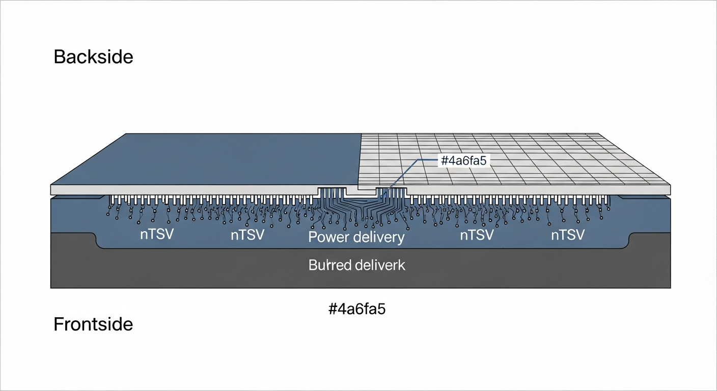
For most of its history, the semiconductor industry has hidden its power distribution in plain sight—stacked on the frontside of the wafer, fighting signal wiring for the same congested real estate above the transistors. Backside Power Delivery Networks (BSPDN) break that convention. By relocating the power rails to the underside of a radically thinned wafer and connecting them to the device layer through nano-scale through-silicon vias (nTSVs), foundries expect to decongest signal routing and cut resistive losses on the power net.
The headline benefits are real, and the roadmaps are firm. Intel has published silicon-validated results under the PowerVia brand. TSMC targets production of its A16 node with Super Power Rail in late 2026, and Samsung has scheduled its SF2Z node for mass production in 2027.
But there's a story that gets under-told—and it's the one that decides whether any of this ships in volume. BSPDN doesn't simply move the power rails. It manufactures an entirely new class of buried, optically inaccessible defects, across four new process steps that didn't exist in a frontside-only flow. So this article treats BSPDN as what it actually is on the fab floor: a yield-recovery problem.
Who this is for: process engineers, silicon-adjacent hardware engineers, and technical product managers who want a synthesis beyond the "clean architectural win" framing—and beyond the single-failure-mode papers that examine one new defect mechanism at a time.
Why Move Power to the Back
It starts with congestion. In a conventional advanced-node processor, power must traverse fifteen or more layers of interconnect to reach the transistors, sharing the frontside stack with the signal network the whole way down. Power and signal lines compete for routing space, and every layer the power net crosses adds resistance and voltage drop.

BSPDN separates the two concerns physically. Power distribution moves to the backside of the wafer, where the rails can be made slightly wider and less resistive than their frontside equivalents. That frees the frontside for signal routing alone. According to figures reported by Semiconductor Engineering, delivering power through these fatter backside lines can reduce power losses on the order of 30 percent through reduced voltage drop—though it's worth noting the measurement conditions and the specific device behind that figure weren't tied to a primary paper, so treat it as a directional headline rather than a spec.
The decongestion effect is where the numbers get more concrete. imec's research ties BSPDN to greater than 90 percent cell utilization in sub-2nm nodes—a direct consequence of clearing power wiring out of the signal planes. Paired with buried power rails (BPR), the same approach is expected to push standard cell heights below the 6-track threshold, a scaling lever that the frontside-only flow had largely exhausted.
This is the natural sequel to the transistor-architecture transition. If gate-all-around nanosheets are the new device, BSPDN is the new wiring beneath it. (See our earlier coverage of the GAA/nanosheet transition and the fundamentals of IR drop and power integrity, both of which set up the payoff described here.)
The PPA case, at the node level, is best illustrated by Samsung's public figures for SF2Z. Speaking at an industry EDA forum, Samsung indicated that BSPDN reduces its 2nm chip area by 17 percent, with performance improving 8 percent and power efficiency 15 percent relative to a traditional frontside power delivery approach. One necessary caveat: these figures come from an executive keynote reported through trade press, not from a primary Samsung technical paper. They describe a roadmap target, not shipped silicon.
Intel is furthest along in the peer-reviewed record. Its PowerVia work has been published through IEEE, and Intel has separately demonstrated 3D-stacked CMOS transistors combined with backside power and direct backside contact. That combination—backside power as the substrate for vertical integration—matters more than it first appears, and we return to it below.
The Reframe: Four New Ways to Lose a Die
Here's the part the architecture-first coverage tends to skip. Every advantage above is purchased with process steps that didn't exist before, and each one is a new source of defects. The frontside stack, for all its congestion, is optically accessible and mature. The backside power net is neither. It's buried beneath the device layer, invisible to frontside inspection, and it depends on operations—wafer thinning, wafer-to-wafer bonding, and via formation at extreme via counts—that push existing fab tooling to its limits.

As one Semiconductor Engineering analysis put it, backside power delivery introduces "a slew of processing challenges, including lithography corrections for distortions due to extreme wafer thinning and bonding of wafer backside to frontside, the latter of which contain millions of nanoTSVs per chip."
Millions of vias per chip. That single figure reframes the entire yield discussion. So consider each new failure mode not in isolation—the way the specialized literature treats them—but as variables in one integrated yield model.
1. Extreme wafer thinning
To expose the device layer to the backside, the wafer has to be thinned to near the transistor plane. This is a high-severity risk, and the technical barrier is threefold: maintaining thickness uniformity across the entire wafer, managing the lithography overlay distortion that thinning induces, and controlling the mechanical stress that comes with removing most of the substrate.
None of these are cheap to mitigate. The mitigation path runs through advanced real-time metrology for thickness control, deliberate stress engineering, and novel thinning processes—each carrying high capital expenditure and a steep yield-learning curve. A processing study on pure-ruthenium nTSV formation and extreme all-dry SOI wafer thinning shows just how specialized the thinning route has become. The fact that a dry-thinning approach warrants its own study is itself a signal of how far this departs from established practice.
2. Wafer-to-wafer bonding defectivity
Thinning requires a bond—the frontside must be bonded to a carrier, and in stacked configurations, wafer to wafer. This is equally high-severity. The failure mechanisms are the classic enemies of any bonding step, now applied across an entire wafer that must be defect-free: particle contamination, void formation, insufficient bond strength, and precise alignment over a large area. A single void or trapped particle is a cluster of dead dies.
The mitigation stack is demanding: ultra-cleanroom environments, high-precision hybrid bonding equipment, and in-situ defect inspection during the bond itself. The market barrier is the corresponding capital investment in bonding tools and the reliability risk during early node ramp, when the learning curve is steepest.
3. nTSV defectivity
This is the defect class that most distinguishes BSPDN from anything that came before. With millions of nano-through-silicon vias per die, each via is a potential open or short, and collectively they introduce resistance variation across the power net. The technical barriers—high-aspect-ratio etching, material compatibility, and etch control at scale—compound because the defects are statistical. You aren't fighting one bad via. You're managing a defect-density distribution across a population large enough that even a very low per-via failure rate translates into meaningful die loss.
This is where the ruthenium work becomes relevant: the mitigation path runs through optimized metallization processes, advanced etch control, and—critically—design-for-test structures. Ruthenium as an nTSV fill material isn't an aesthetic choice. It's a defectivity-and-resistance choice.
4. Disrupted thermal path
The fourth risk is medium-severity but strategically important. Moving power delivery to the backside changes the heat-removal path. The silicon substrate that once conducted heat away from the transistors is thinned or displaced, raising the specter of localized hot spots and elevated junction temperatures. The existence of this thermal barrier is well sourced; the precise magnitude of the junction-temperature penalty is not, so we resist quoting a number here.
What matters for yield and reliability is that thermal can no longer be solved after the fact. Mitigation forces thermal co-design early, coupling to advanced packaging solutions such as direct backside contact and, potentially, liquid cooling integration.
The unified picture
Read individually, each of these is a manageable engineering problem with a known mitigation path. Read together, they describe a fundamentally harder proposition: a buried power network whose defects can't be seen from the frontside, formed by thinning, bonding, and via steps that each carry their own defect-density budget, under a thermal constraint that pulls packaging into the design loop. Yield recovery at 2nm is the sum of these four learning curves converging at once.
Where the Foundries Stand
The three leading-edge foundries have converged on BSPDN but diverged on branding and timing. Intel's PowerVia reached silicon first, with results published through IEEE and IEDM. TSMC's Super Power Rail is slated for its A16 node, with production targeted for the fourth quarter of 2026. Samsung's BSPDN debuts on SF2Z, with mass production targeted for 2027.
A note on confidence: the production-timing targets for A16 and SF2Z carry high confidence as stated roadmap commitments. Secondary trade press has attached specific PPA deltas to A16 relative to TSMC's N2 node, but those figures weren't confirmed against a TSMC primary technical disclosure, and we decline to state them as fact. Samsung's timing should be read the same way—roadmap-stated rather than shipped. At least one industry commentator has publicly questioned the maturity of Samsung's volume BSPDN design pipeline.
The through-line is that all three are climbing the same four learning curves described above, on their own process routes. That's precisely why no single-vendor paper generalizes the yield-recovery problem—and why an integrated view is useful.
Speculation: Yield Learning as a Transferable Asset
The following is fact-based speculation, grounded in dossier-cited trajectories and labeled as such.
Speculation: BSPDN yield learning transfers directly to 3D-SOC integration. imec explicitly frames backside power delivery as extending beyond 2D single-die ICs into 3D systems-on-chip. If that framing holds, then the thinning, bonding, and nTSV toolset developed to recover BSPDN yield is largely the same toolset required for logic-on-logic and memory-on-logic 3D stacks. The implication? The painful, capital-intensive learning curve foundries are climbing now isn't a one-generation cost—it's an investment whose returns compound across product families. Intel's demonstration of stacked CMOS combined with backside power and direct backside contact is the earliest concrete evidence pointing this direction. (Grounded in the imec 3D-SOC statement and Intel's stacked-CMOS demonstration; the forward inference is speculative.)
Speculation: yield recovery becomes a metrology and DFT problem, not only a process problem. With millions of nTSVs and no frontside optical access to the buried power net, defect localization shifts toward electrical inference and on-die monitoring. That favors design-for-test structures and embedded power-net monitors as first-class citizens of the design flow rather than afterthoughts. (Speculative, grounded in the nTSV defectivity risk and DFT mitigation path.)
Speculation: thermal co-design pulls packaging forward in the schedule. Because the substrate heat path is disrupted, thermal can no longer be validated late. The likely consequence is earlier, tighter coupling between device design and advanced packaging—direct backside contact today, near-junction and liquid cooling further out. This reinforces the 3D-SOC thesis: the same backside toolset that enables stacking also concentrates heat that packaging must then remove. (Speculative, grounded in the thermal-dissipation risk.)
The Takeaway
BSPDN is often presented as a clean architectural win: relocate the rails, decongest the frontside, cut IR drop, shrink the cell. Each of those benefits is real and quantified—up to 30 percent lower power loss in reported figures, greater than 90 percent cell utilization, sub-6T cell heights, and node-level PPA gains in the mid-teens percentages on Samsung's roadmap.
But the benefits aren't the constraint. Yield is. BSPDN introduces four new, largely simultaneous ways to lose a die—extreme thinning, wafer bonding, nTSV defectivity, and a disrupted thermal path—three of them rated high-severity, all of them producing defects that the frontside inspection infrastructure was never built to see. The path to 2nm yield recovery runs through the convergence of those four learning curves. And the foundry that climbs them fastest owns more than a node. If the 3D-SOC trajectory holds, it owns a transferable manufacturing capability that outlives any single generation.
Forward links: our upcoming deep dives on 3D-SOC and hybrid bonding, advanced-packaging thermal co-design, and design-for-yield in the angstrom era each pick up a thread seeded here—the bonding-and-thinning toolset as a bridge to stacking, the packaging-thermal coupling, and the buried-defect metrology problem, respectively.
Sources
- The Best-Kept Secret in Semiconductor Innovation: Backside Power Delivery — McKinsey Electronics, 2025
- Backside Power Delivery Gears Up For 2nm Devices — Semiconductor Engineering, 2024
- Challenges In Backside Power Delivery — Semiconductor Engineering, 2024
- Backside Power Delivery Creates Fab Tool, Thermal Dissipation Barriers — Semiconductor Engineering, 2024
- How to power chips from the backside — imec, 2024
- Samsung's Backside Power Delivery Network Reportedly to Reduce 2nm Chip Size by 17% — TrendForce, 2024
- TSMC Is On Track for A16 Mass Production in Late 2026 with Advanced Backside Power Delivery — TrendForce, 2024
- Intel PowerVia Technology: Backside Power Delivery for High Density and High-Performance Computing — IEEE Xplore (document 10185208), 2023
- Intel demos first 3D stacked CMOS transistors combined with backside power and direct backside contact — Semiconductor Today, 2023
- PowerVia Test Shows Industry-Leading Performance — Intel, 2023
- Pure Ru n-TSV Processing and Extreme All-Dry SOI Wafer Thinning for a Backside Power-Delivery Network — ResearchGate (record 397293655), 2024–2025
Stay in the loop. Project Isocline publishes deep-dive technical analysis on AI infrastructure, energy systems, and the engineering decisions shaping the next decade of compute. No noise. No fluff.
You can unsubscribe at any time.