Ferroelectric HfO₂ Memory: How a 2011 Crystallographic Accident Turned the Standard Gate Dielectric Into a Compute Substrate
At a Glance
For most of its life, ferroelectric memory has been a technology of footnotes — promising, but stranded on exotic materials like lead zirconate titanate (PZT) that no logic fab wanted anywhere near its process line. Then, in 2011, a structural investigation of silicon-doped hafnium oxide turned up something that shouldn't have been there: a stable, non-centrosymmetric orthorhombic phase in the industry's single most ubiquitous gate dielectric.
That discovery reframed the whole problem. Ferroelectricity was no longer something you had to bolt on with unfamiliar elements. It was already latent in a material sitting inside every modern high-k metal gate (HKMG) transistor. And that's the strategic shift this article is about: the ferroelectric field-effect transistor (FeFET) is quietly graduating from a memory-replacement candidate into a non-volatile compute substrate — one that rides on the existing gate module instead of demanding a new device architecture.
The short version of the argument:
- The switchable polarization originates in the Pca2₁ orthorhombic phase of doped HfO₂ — a phase deviation first documented by Böscke et al. in 2011.
- Because the ferroelectric is just doped hafnium oxide, integration has already reached the 22 nm FD-SOI node, with embedded-NVM arrays demonstrated at 28 nm HKMG.
- The frontier is no longer storage. Silicon-validated compute-in-memory (CiM) macros now report 346.6 TOPS/W for binary multiply-accumulate, and FeFET-based combinatorial-optimization engines report 75% chip-area savings on Max-Cut problems.
- The gating question is reliability, not physics: demonstrated embedded parts have shown endurance up to 100,000 cycles, and commercialization remains an open contest against MRAM, PCM, and ReRAM.
This piece traces one continuous line — from a 2011 materials accident, through CMOS integration, to today's compute demonstrations.
1. The Materials Accident That Started It
To understand why FeFETs matter now, you have to start with why they didn't matter before.
Classical ferroelectrics are perovskites — PZT and its relatives. They switch beautifully. But they carry lead and other non-standard elements into the fab, and their properties degrade as you scale them toward modern film thicknesses. For a logic foundry, integrating them is less an engineering task than a contamination-control nightmare. So ferroelectric memory lived at the margins.
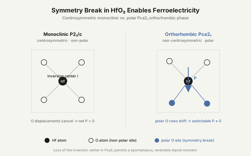
The 2011 discovery changed the material, not just the device. Detailed structural and electrical investigations of Si-doped HfO₂ thin films by Böscke et al. revealed deviations from the commonly assumed monoclinic–tetragonal–cubic polymorphism, leading to the rediscovery of an intermediate orthorhombic phase. That non-centrosymmetric phase — space group Pca2₁ — is the physical origin of switchable polarization. In plain terms: a symmetry break in the crystal lattice lets the material hold one of two stable polarization states without power, and lets you flip between them with a voltage.
Two properties made this a strategic event rather than a curiosity. First, these hafnia-based ferroelectrics have a completely different crystal morphology from conventional perovskites, and they present more robust ferroelectric properties as you scale them aggressively — the exact opposite of the perovskite problem. Second, and this is the decisive one, they're compatible with standard integrated-circuit fabrication.
The design philosophy that follows is worth stating outright, because it's the entire thesis of the technology: the goal is to leverage the properties of ferroelectric hafnium oxide rather than to create a new device architecture using exotic materials. Everything downstream — the node milestones, the compute macros — falls out of that single decision.
Backward link: This is the natural sequel to our earlier discussion of embedded flash hitting a wall below 28 nm. If eFlash can't follow logic scaling, the replacement that reuses the existing gate module is the one to watch.
[LINK: The Death of Embedded Flash Below 28 nm]
2. How a FeFET Actually Works
A FeFET is a three-terminal, non-volatile device that stores data as a permanent, switchable shift in the transistor's threshold voltage. Structurally it's a MOSFET with one substitution: a ferroelectric oxide layer sits in the gate stack. The canonical form is the metal–ferroelectric–insulator–semiconductor (MFIS) stack, where doped HfO₂ is the ferroelectric layer.
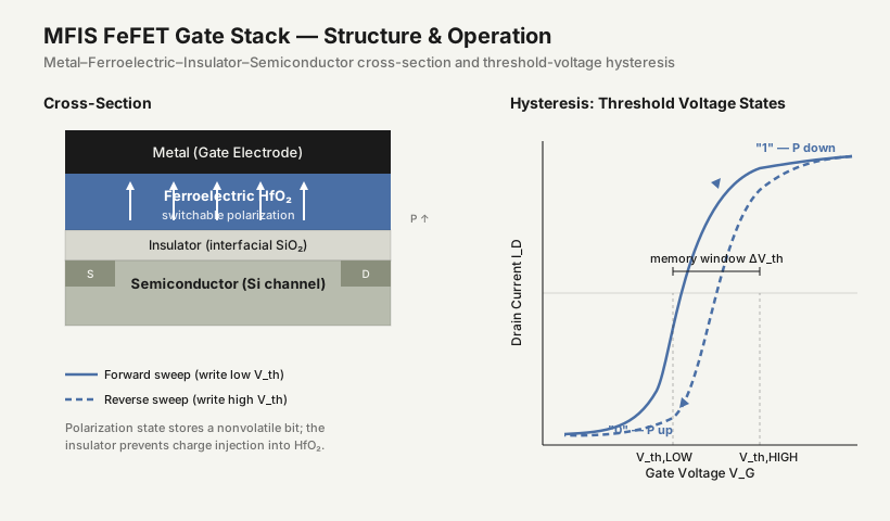
The non-volatility comes from a capacitance coupling. The ferroelectric capacitance (C_FE) couples with the capacitance of the underlying MOSFET (C_CMOS). The hysteresis that arises from this coupling is what makes the device remember. When the ratio C_FE/C_CMOS is low enough, the polarization state is retained, producing a hysteresis curve — and that hysteresis is the memory window separating the two logic states.
For compute, the architectural fact that matters is the separation of read and write paths that a three-terminal device gives you. Reading senses the drain–source current; writing switches the ferroelectric polarization with an appropriate gate–source voltage. And the consequence for energy is enormous: unlike two-terminal variable-resistance devices, a FeFET doesn't require a drain–source current during writing. You're reorienting dipoles with a field, not pushing current through a filament. That's the root of its low write energy — and, as we'll see, the root of its appeal as a compute element where write energy dominates.
The early device confirmed the whole proposition was viable. Böscke's 2011 CMOS-compatible FeFET used an 8.5 nm ferroelectric layer annealed at 1000 °C (which produced a 1.2 nm SiO₂ interlayer). A short-channel device of 150 nm × 80 nm achieved a memory window up to 1 V and demonstrated ten-year non-volatile retention. The physics worked. The question was whether it would survive a real process node.
3. From Physics to Process Node
It did. The migration from lab film to logic node is the part of this story that sets FeFET apart from most emerging-memory research — and it happened faster than the norm.
In 2012, Müller et al. fabricated a Si:HfO₂ FeFET in 28 nm HKMG technology — using the hafnium-based ferroelectric specifically because of its process scalability, which is what made the 28 nm node accessible in the first place. Operation was proven down to a 28 nm gate length, with program/erase, endurance, and retention characterized for gate lengths scaled to 32 nm.
The path to a manufacturable embedded NVM was carried largely by a consortium: Fraunhofer, GlobalFoundries, and NaMLab began exploring FeFETs in 2009, with FMC later spun out of NaMLab. By 2014 the group had demonstrated a simple FeFET array on a 28 nm CMOS process. Then a pivotal integration result landed in 2016: a FeFET-based eNVM built into a 28 nm HKMG (28SLP) CMOS platform, in which the electrical baseline properties of the platform stayed unchanged by the FeFET integration. That JTAG-controlled 64 kbit memory showed clearly separated states, demonstrated high-temperature retention, and reached endurance up to 100,000 cycles.
The milestone that best captures the CMOS-compatibility thesis came in 2018: the consortium demonstrated an embedded, non-volatile FeFET in a 22 nm FD-SOI process. The significance isn't any single specification. It's that the ferroelectric memory layer was made to ride on top of a production logic platform without disturbing the transistors underneath it. That's the "free NVM layer on the gate stack" argument, realized in silicon.
Sidebar — Continuity for the memory-comparison reader: Placed against MRAM, ReRAM, and PCM, FeFET's distinguishing column is the low-write-energy, three-terminal architecture — no write current, separate read/write paths. That's the differentiator worth carrying into any emerging-NVM comparison.
[LINK: Emerging NVM Shootout — MRAM vs. ReRAM vs. PCM]
4. The Turn: From Memory to Compute
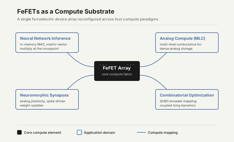
Here's where the narrative pivots — and where the accessible literature has largely not yet followed. Most explanatory coverage frames FeFET as a memory contender, an embedded-flash successor. The more consequential development of the last three years is its emergence as a compute substrate. Among the various emerging NVMs, HfO₂-based FeFETs have recently surfaced as an appealing candidate for non-volatile logic — and, built on rich electrostatic physics and high CMOS compatibility, they've been applied to memories, ternary content-addressable memories (TCAMs), and binarized convolutional neural networks.
The compute-in-memory (CiM) case rests on the same physical fact from Section 2: no drain current during write. Combine that with a high Ion/Ioff ratio and a low read voltage, and FeFET becomes a strong fit precisely where two-terminal resistive devices struggle — write energy and sneak-path currents.
Neural-network inference. A recent macro makes the efficiency concrete. Fabricated in the GlobalFoundries 28 nm HKMG process, it comprises a 64×64 FeFET array with peripheral circuitry for program, erase, and current-mode CIM operations, plus eight 4-bit Flash ADCs. It achieves an energy efficiency of 346.6 TOPS/W for 1×1-bit multiply-accumulate, and an inference accuracy of 85.2% (16-row parallel compute, 4-bit ADC) against a 89.7% software baseline on VGG-8 for CIFAR-10.
Analog compute via multi-level cells. Beyond binary operation, multi-level-cell (MLC) operation of AND-connected FeFET arrays suits analog CiM. One study reported a 4% bit-error-rate in inference-only operation — only a 1% degradation from floating-point accuracy for CIFAR-10 with LeNet.
Neuromorphic synapses. FeFETs make strong synaptic devices because of multi-level programmability, non-volatility, and CMOS compatibility. Multi-bit synapse operation was demonstrated experimentally on GlobalFoundries' 28 nm CMOS using an incremental-pulsing scheme, showing stable access to intermediate polarization states with long-term retention. At the system level, a 28 nm HKMG FeFET crossbar reached software-comparable ~97% accuracy on MNIST with a multilayer perceptron.
Beyond MAC — combinatorial optimization. The most architecturally interesting result pushes past neural inference entirely. A FeFET-based CiM annealer solves combinatorial optimization problems by converting them to QUBO formulations and accelerating the core vector-matrix-vector (VMV) multiplication in situ, in a single step. The three-terminal FeFET structure permits lossless compression of the stored QUBO matrix, yielding a 75% chip-size saving when solving Max-Cut problems — and it was experimentally validated on the first integrated FeFET chip built in 28 nm HKMG CMOS.
The through-line across all four is that none of them needed exotic substrates. Every one of these results runs on a production-class HKMG node. And that's the differentiation: FeFET offers a VLSI-compatible route to compute paradigms — including Ising-style optimization — that usually demand specialized hardware.
Forward link: The 346.6 TOPS/W macro and the MLC crossbar results deserve a dedicated benchmarking treatment against other CiM approaches for edge inference.
[LINK: Compute-in-Memory Accelerators for Edge AI]Forward link: The QUBO annealer earns FeFET a place in a broader taxonomy of solver hardware.
[LINK: Ising Machines & QUBO Hardware]
5. What the Patents Reveal
The patent record is worth reading — not for legal detail, but because it confirms industry framed HfO₂ ferroelectricity, from the outset, as a process-alignment play rather than a materials-science novelty.
One USPTO-published patent states the compatibility argument almost verbatim: since HfO₂ is typically used as the gate dielectric in CMOS, a ferroelectric layer serving as the gate dielectric in an embedded memory cell yields very compatible processing with the baseline CMOS — and if a doped-HfO₂ layer were also used for the CMOS logic, the result would stay quite compatible while additionally offering a steeper subthreshold slope. The same filing describes a NOR-array embedded memory built from ferroelectric memory FETs paired with select devices.
A second patent documents the mechanism candidly, and that candor is instructive. It attributes the ferroelectric behavior of certain hafnium-based materials — as opposed to the paraelectric nature of hafnium-rich compositions — to an appropriate crystalline state established in suitably doped hafnium oxide. Crucially, it notes that while hafnium-oxide ferroelectrics may be expected to show better CMOS compatibility, several drawbacks show up in actual implementations. The IP record itself flags what everyone eventually learns: the physics is easier than the manufacturing.
Finally, the compute angle is now protected: a patent covers using FeFETs as capacitive processing units for in-memory computing, describing a grid of word lines and bit lines with in-memory processing cells at the intersections, each built from two switches and a non-volatile tunable capacitor. The compute framing isn't speculative journalism. It's codified intellectual property.
(A note on provenance: the current assignee ownership and patent-family scope for the specific filings referenced here could not be independently confirmed for this article and should not be treated as settled.)
6. The Reliability Question — Stated Honestly
No credible account of FeFET can end on the compute high note without confronting why it isn't yet everywhere. The barriers are engineering and market, not physics.
Endurance. Demonstrated embedded parts have reached endurance up to 100,000 cycles. The literature ties endurance ceilings to charge trapping and dielectric breakdown at the interfacial layer between the ferroelectric and the semiconductor. Call this a medium-severity risk: it doesn't preclude adoption, but it constrains use cases that require frequent, high-volume writes. The mitigation paths are material engineering — the migration toward hafnium-zirconium oxide (HZO) and alternative dopants (Si, Zr, Al, Y, and Ga have all been reported) — along with interface optimization and revised device architectures.
(A caution for practitioners: generalized endurance limits vary by study and device, and a single canonical figure for the FeFET class shouldn't be assumed. Treat 100,000 cycles as a demonstrated embedded-NVM result, not a universal ceiling.)
Device variability. Non-uniformity in ferroelectric properties across devices affects the memory window and threshold voltage — a medium-severity risk that complicates high-yield manufacturing and large-array integration. Mitigations run from process optimization and better characterization to circuit-level compensation.
Commercialization uncertainty. This is the high-severity risk. The technology remains substantially in R&D. Industry commentary has framed the open question directly: GlobalFoundries has pursued a 28 nm/22 nm logic-compatible FeFET process for embedded memory using FDSOI to reduce power, but whether FeFETs and next-generation ferroelectric memories will ever reach volume production remains unclear — especially because competing new memories (MRAM, PCM, ReRAM) are already in the market. The materials advantage is real. The market window is contested.
7. Where This Goes Next
Speculation (grounded in dossier-cited trajectories): The cleanest way to read FeFET's future is as a logic-compatible eNVM that arrives essentially for free on the gate stack. The framing in the literature is explicit — harnessing the polar orthorhombic Pca2₁ phase in doped hafnium oxide, you can build a one-transistor non-volatile ferroelectric memory that serves as a logic-compatible, high-performance embedded NVM. As embedded flash struggles below 28 nm, a single-transistor cell that reuses the existing HKMG gate module is a natural complement to logic-scaling roadmaps rather than a competitor to them.
Speculation: The stronger long-term thesis is architectural convergence. FeFET is already cataloged inside the broader compute-near-memory and compute-in-memory research landscape. Its low write energy and high Ion/Ioff make it a candidate for placing non-volatile weight storage directly adjacent to logic — and, combined with chiplet and 2.5D packaging, for attacking the von Neumann data-movement penalty that motivates the entire CiM field. The demonstrated QUBO annealer suggests the reach extends past neural inference into dynamical optimization hardware — but on standard silicon rather than exotic substrates.
Speculation (materials divergence): A longer-horizon branch sits outside the HfO₂ story proper. Laterally-gated FeFETs using van der Waals channels such as α-In₂Se₃ have been proposed for stacked in-memory computing arrays. These are not HfO₂-based and belong in a separate lineage, but they hint at where density and 3D integration could go if the AND-connected-array approach — already shown to be fabricable in both 28 nm HKMG and 22 nm FD-SOI — scales vertically in the manner of NAND.
There's one more thread worth pulling. The dopant search that keeps HfO₂ ferroelectricity alive is increasingly a computational-materials problem — machine-learning-driven phase-stability evaluation has been used to identify new dopants such as gallium in hafnium oxide. That connects this hardware story to a different domain entirely.
Forward link: The FeFET-PUF work built on this same 28 nm / 22 nm substrate connects it to a hardware-security narrative.
[LINK: Hardware Root-of-Trust for IoT]Forward link: The ML-driven discovery of new hafnia dopants bridges this piece to a computational-materials thread — a strong cross-domain "why now."
[LINK: AI for Materials Discovery]
Closing
The FeFET story is unusually clean for an emerging-hardware narrative. It begins with a single crystallographic finding in 2011 — the Pca2₁ orthorhombic phase in doped hafnium oxide — and that one fact propagates all the way through. It's why integration reached 22 nm FD-SOI without disturbing the baseline transistors. It's why compute macros run on production HKMG silicon. It's why the whole value proposition boils down to reusing the gate module you already have.
What's changed recently is the frame. FeFET is no longer just a memory contender waiting to displace embedded flash. Silicon-validated CiM macros, MLC crossbars, neuromorphic synapses, and a QUBO annealer have quietly relocated it into the compute layer. Whether it wins the commercial contest against MRAM, PCM, and ReRAM is genuinely unresolved, and the endurance and variability questions are real. But the underlying bet is coherent and — unusually — materials-cheap: turn the industry's standard gate dielectric into non-volatile compute, and let it ride the logic roadmap it was already part of.
Stay in the loop. Project Isocline publishes deep-dive technical analysis on AI infrastructure, energy systems, and the engineering decisions shaping the next decade of compute. No noise. No fluff.
You can unsubscribe at any time.