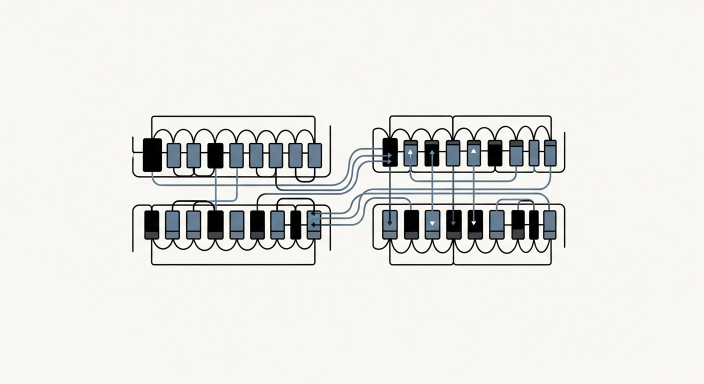
Analog In-Memory Computing for Transformer Attention: The Charge-Domain Revival
At a Glance
Every autoregressive token a transformer generates kicks off the same expensive ritual. Pull the cached key and value projections out of memory, load them into fast on-chip SRAM, compute the attention dot-products, and write the new token's projection back. The weights never change during inference. The KV cache does — every single step. That mutability is the crux of the whole problem, and it's the reason a decades-old idea from the DRAM world is being resurrected for the most modern workload in computing.
A cluster of 2024–2025 results has shown something surprising: attention dot-products can be computed inside the memory that stores the KV cache, using capacitor-based gain cells that work in the charge domain rather than the current domain. The flagship result, from Forschungszentrum Jülich and RWTH Aachen, reports attention latency cut by up to two orders of magnitude and energy by up to four orders of magnitude versus GPUs. A separate 65 nm silicon prototype proves the concept in measured hardware. IBM, coming at it from a different angle, sidesteps analog softmax entirely through kernel approximation.
This piece is organized around a single thesis that the existing coverage — dense academic papers and vendor blogs — largely leaves implicit: the writability of charge-domain memory is what makes it the natural substrate for attention, and it is precisely what disqualifies the resistive memories better suited to static weights.
Why Attention, Specifically, Is the Hard Part
In-memory computing has a well-understood value proposition for the static portion of a neural network. Weights are fixed after training. You program them once into a memory array, stream activations through it, and let Ohm's law and Kirchhoff's law perform the matrix-vector multiplication physically. This is the analog AI story that resistive memories — ReRAM, PCM, FeFET — have chased for years. Program the conductance once, amortize the write cost over billions of inferences.
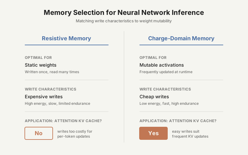
Attention breaks that assumption. During generative inference, self-attention uses a cache to store token projections so it doesn't have to recompute them at every step. But those cached projections aren't static weights. Each new token appends fresh keys and values to the cache, and on conventional hardware the entire cache has to be reloaded into SRAM for every generation step. This repeated movement — not the arithmetic itself — dominates latency and energy. It's the von Neumann bottleneck showing up at the exact layer that defines the transformer.
That reframes the substrate question. If your in-memory array has to be rewritten every token, then write speed, write energy, and write endurance become first-order constraints, not afterthoughts. Resistive memories are optimized for the opposite regime: expensive, occasional writes amortized over long read-dominated lifetimes. HARDSEA, a hybrid analog-ReRAM clustering and digital-SRAM accelerator for dynamic sparse self-attention, illustrates the resistive path — but the substrate is fundamentally more comfortable holding something that doesn't change.
Charge-domain gain cells invert that tradeoff. They're easy to write. And that single property is why they've re-emerged as the substrate of choice for a mutating KV cache.
(For the underlying data-movement argument, see our earlier treatment of the memory wall and the von Neumann bottleneck; this article is that problem's concrete instantiation at the attention layer.)
The Charge-Domain Revival: An Old Idea, Recontextualized
The novelty here isn't the capacitor. Storing information as charge on a capacitor is the foundational physics of DRAM, and gain cells — small multi-transistor cells that store a value on an internal node and read it out with gain — have a long lineage in embedded DRAM (eDRAM) design.
The classic weakness of any charge-storage cell is retention: charge leaks away, and the cell has to be refreshed. That one limitation is what historically kept charge-domain storage out of applications demanding static-memory reliability. Modern gain-cell engineering attacks it head-on. Recent eDRAM work describes a two-transistor gain cell with pseudo-static leakage compensation that maintains stored data without charge-loss issues, offering unlimited retention time in the same manner as static memory — while a capacitor-free realization using metal-oxide-metal capacitors achieves area reductions of 21% and 42% versus 6T and 8T SRAM cells in the same process. Smaller than SRAM, and now retention-stable.
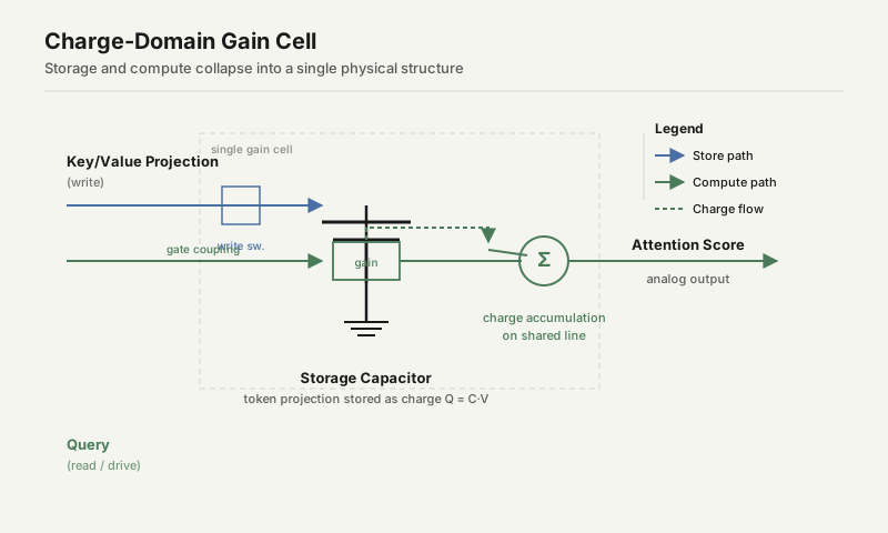
So the revival is really the act of pointing this matured device physics at attention. The gain cell does double duty: it stores a token's projection, and — through charge-domain summation across the array — it computes the dot-product against the incoming query in place. Storage and compute collapse into the same physical structure, and the SRAM reload that dominated the energy budget simply disappears.
The Flagship Result: Gain-Cell Attention
The Jülich/RWTH Aachen architecture replaces the SRAM-based KV cache, and all the data movement it implies, with capacitor-based gain cells that store token projections and perform parallel analog dot-product computation. Newly generated tokens get written into the array as the sequence unfolds; the attention scores are read out as an analog charge-domain operation.
The headline numbers — up to two orders of magnitude lower attention latency and up to four orders of magnitude lower energy versus GPUs — are striking. But the engineering that makes them legitimate is more interesting than the figures themselves.
A note on the energy claim. The original arXiv preprint reported five orders of magnitude energy reduction. The peer-reviewed Nature Computational Science version revises this to four. We treat the peer-reviewed figure — four orders (energy), two orders (latency) — as canonical, and flag the discrepancy because summaries circulating from the preprint may keep propagating the superseded number.
Making a lossy substrate usable
Analog gain-cell circuits are imprecise. They introduce non-idealities and constraints that prevent the direct mapping of a pre-trained model onto the hardware — you can't just take GPT-2's weights, load them into a noisy analog array, and expect equivalent behavior. Rather than retrain from scratch, the authors designed an initialization algorithm that achieves text-processing performance comparable to GPT-2 without training from scratch. This is the pragmatic core of the contribution: an adaptation procedure that reconciles pre-trained model behavior with the physical realities of the substrate.
Reshaping the algorithm to fit the silicon
Two algorithmic pivots make the fixed-size physical array viable.
First, softmax is abandoned. Softmax is notoriously awkward to implement in analog. So the design leans on the finding that other nonlinear activations yield similar accuracy — specifically, sigmoid-based attention has been shown to match softmax-based attention on models up to 7 billion parameters. That decouples the architecture from an operation the substrate handles poorly.
Second, the memory footprint is bounded. Conventional attention's memory requirement scales with sequence length; a physical gain-cell array has finite capacity. Sliding-window attention resolves the mismatch by keeping only the most recent tokens, mapping a bounded working set onto a fixed-capacity array.
The pattern worth internalizing: this is hardware-algorithm co-design, where the attention variant is deliberately reshaped to fit the substrate, not the other way around.
The Hybrid Pattern: Analog Triage, Digital Residual
The most important architectural idea in the field isn't any single accelerator — it's a division of labor that multiple independent groups have converged on.
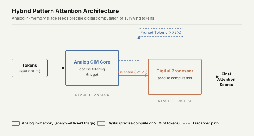
A measured 65 nm CMOS prototype makes it concrete. The analog computing-in-memory core acts as a coarse, ultra-low-power filter, pruning roughly 75% of low-score tokens at runtime. A digital processor then performs precise computation only for the ~25% of unpruned tokens the analog core selected — which prevents the accuracy degradation that pure-analog compute would incur. The measured efficiency reflects the split: peak energy efficiency of 14.8 TOPS/W in the analog core versus 1.65 TOPS/W at the system-on-chip level, with peak area efficiency of 976.6 GOPS/mm² in the analog core against 79.4 GOPS/mm² for the full SoC.
The reasoning is elegant. Attention is dominated by tokens that contribute little; you don't need high precision to identify them, only to rank them. So let noisy, cheap analog physics do the ranking, and spend expensive exact digital compute only where precision actually affects the output.
IBM lands on a structurally similar answer from a different starting point. Its scientists are candid that the attention computation isn't something you can straightforwardly accelerate in analog. Rather than force the issue, IBM reformulates attention through kernel approximation, recasting it as a linear-complexity operation amenable to in-memory execution. IBM also reports an end-to-end milestone: the first deployment of a transformer on an analog in-memory computing chip in which every matrix-vector multiplication involving static model weights runs in-memory, performing within 2% of full floating-point accuracy on the Long Range Arena benchmark.
Two independent teams, two different techniques, one shared principle: use analog charge-domain physics for the approximate majority, and reserve exact digital compute for the precision-critical minority. This is the field's answer to the accuracy-versus-noise problem, and it's the strongest signal available about what near-term hardware will actually look like.
The Patent Landscape
The intellectual-property fencing around charge-domain and eDRAM-based CIM is active and — notably — explicit about the charge-versus-current distinction that organizes this article.
One filing claims a charge-domain compute-in-memory technique based on eDRAM, explicitly differentiated from SRAM-based or current-domain approaches, citing enhanced retention time and high-accuracy, energy-efficient operation (US12105986B2, 2024). That's the substrate thesis, rendered as a patent claim.
Transformer-specific filings are emerging too. One describes an accelerator architecture for a transformer model in which the key matrix, value matrix, and query weight matrix are processed in random-access memory configured for processing-in-memory (US20250028563A1, 2025) — the KV/query structure mapped directly onto the memory array. Adjacent claims cover capacitor-based MAC in-memory cores (US11586896B2, 2023) and charge-sharing schemes that mitigate cell-current variation for accuracy, averaging per-cell capacitors across a column to suppress variation (US20210263672A1, 2021) — a device-level echo of the same noise-tolerance strategy the hybrid architectures pursue at the system level. A separate application targets transformer workloads via in-memory compute chiplets (US Patent Application 20240160586, 2024).
One caveat on concentration. A patent-analytics vendor characterizes a single leading assignee as dominant across eDRAM CIM macros, analog CIM with charge reuse, and attention-fusion PIM. We couldn't confirm that assignee's identity or filing counts against primary USPTO or Google Patents records, so we present it only as vendor-reported rather than established fact.
Speculation: Where This Goes
The following is synthesis grounded in the dossier's cited trajectories, not sourced fact, and is labeled accordingly.
Speculation: The near-term commercial artifact is a co-processor, not a monolithic analog LLM chip. Both the silicon prototype and IBM's kernel-approximation path point away from pure-analog systems. The plausible product is a charge-domain KV-cache co-processor bolted onto a conventional digital NPU — handling the mutable, movement-heavy attention cache in analog while the digital fabric keeps everything precision-sensitive.
Speculation: Attention variants and hardware will keep co-designing, favoring bounded-state models. The reliance on sigmoid and sliding-window attention already shows the algorithm bending to fit the substrate. Models whose state is bounded and recurrent — linear-attention and state-space architectures — map cleanly onto a fixed-capacity gain-cell array, and are the natural candidates to become preferred targets. This is our extrapolation from the co-design pattern, not a claim any cited work makes directly.
Speculation: Retention engineering is the gating variable for context length. Because the cache is rewritten every token, gain-cell write speed and endurance, together with leakage-compensation schemes like pseudo-static cells, will bound the maximum practical context before refresh overhead erodes the energy advantage.
Speculation: The edge is the beachhead. A four-orders-of-magnitude energy reduction matters most where power, not throughput, is the binding constraint — always-on assistants, wearables, intelligent sensor nodes — well before data-center adoption becomes the story.
The Takeaway for System Designers
The energy headline is real, but it's the wrong thing to lead with. The durable insight is architectural: attention's KV cache is a mutating store, and that mutability selects the memory substrate. Charge-domain gain cells win not because they compute dot-products more elegantly than resistive alternatives, but because they're easy to write — and a cache that changes every token demands exactly that. The resistive memories that excel at holding static weights are, for this specific workload, solving the wrong problem.
The second insight is that nobody serious is betting on pure analog. The convergent hybrid pattern — analog triage, digital residual — is the field's mature response to the noise problem, and it's the shape near-term hardware will most likely take.
The softmax-to-sigmoid pivot is a rich enough story to stand on its own, and we intend to return to it in a dedicated look at softmax-free transformers. The transformer CIM-chiplet filings likewise open onto a broader question of packaging and integration for AI accelerators — a thread we plan to pick up in future coverage of chiplet architectures.
Sources
- Leroux et al., "Analog in-memory computing attention mechanism for fast and energy-efficient large language models," Nature Computational Science, 2025.
- Leroux et al., preprint, arXiv:2409.19315, 2024.
- Moradifirouzabadi et al., "An Analog and Digital Hybrid Attention Accelerator for Transformers with Charge-based In-memory Computing," arXiv:2409.04940, 2024.
- IBM Research, "Analog in-memory computing could power tomorrow's AI models," 2025; and "Kernel approximation using analogue in-memory computing," Nature Machine Intelligence, 2024.
- Liu et al., "HARDSEA," IEEE TVLSI 32, 269–282, 2024.
- "Pseudo-Static Gain Cell of Embedded DRAM for Processing-in-Memory in Intelligent IoT Sensor Nodes," MDPI Sensors 22(11):4284, 2022.
- Patents: US12105986B2 (2024); US20250028563A1 (2025); US11586896B2 (2023); US20210263672A1 (2021); US Patent Application 20240160586 (2024).
Stay in the loop. Project Isocline publishes deep-dive technical analysis on AI infrastructure, energy systems, and the engineering decisions shaping the next decade of compute. No noise. No fluff.
You can unsubscribe at any time.