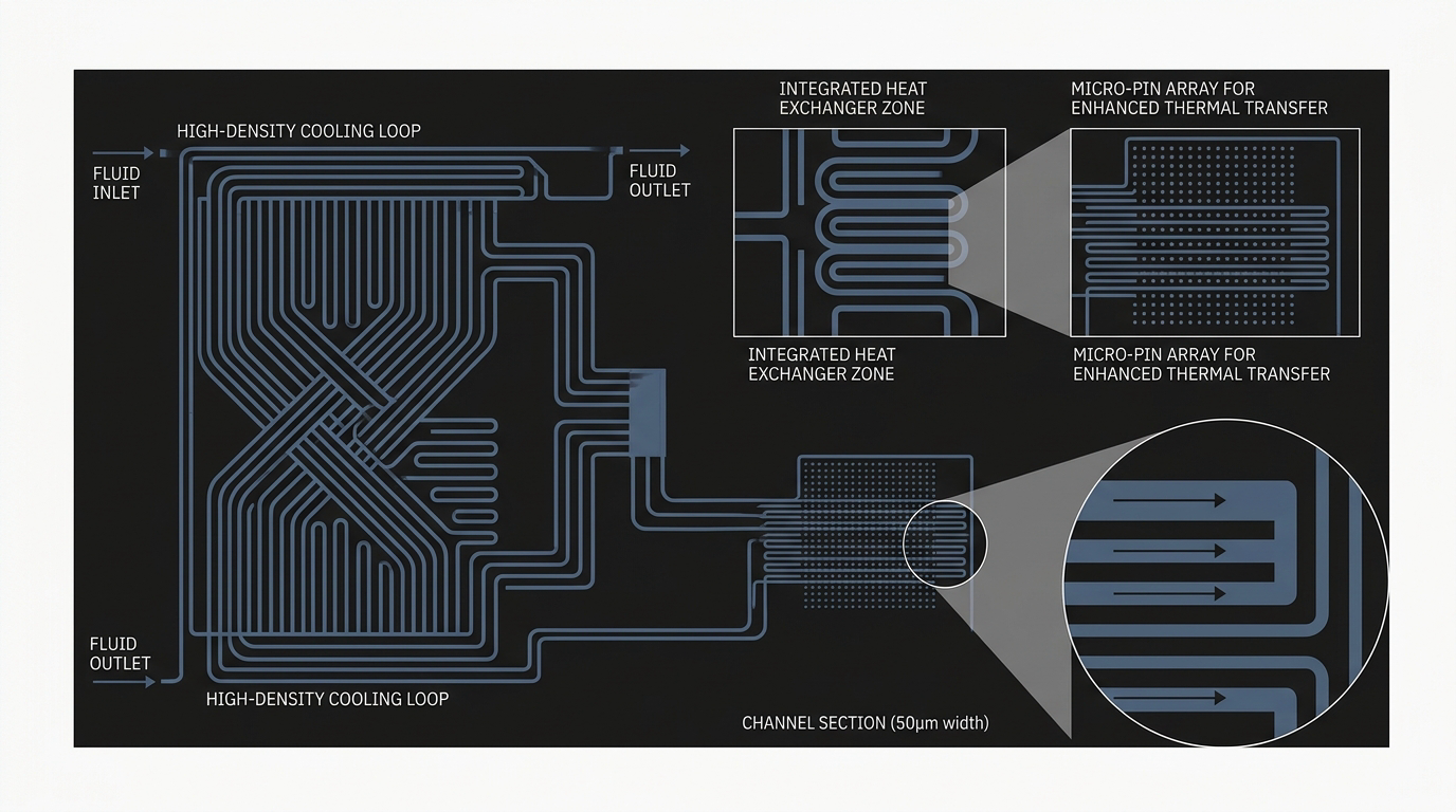
Cooling From Inside the Silicon: Microfluidics and the Thermal Wall in 3D-Stacked Chips
At a Glance
- The problem: Stacking memory directly on a processor shortens wires and raises bandwidth, and it also traps heat. In a 2025 imec model, putting high-bandwidth memory straight on top of a GPU pushed peak GPU temperature to 141.7 °C, against 69.1 °C for the same parts side by side.
- The old idea: Etching coolant channels into silicon dates to 1981, when Tuckerman and Pease removed 790 W/cm² with a 71 °C temperature rise. IBM cooled a 3D stack with water flowing between layers in 2008, and DARPA's ICECool program set out in 2012 to demonstrate more than 1 kW/cm².
- What's changed: The idea is moving into production packaging. TSMC fusion-bonds a microchannel silicon cooler straight to the die backside on its CoWoS platform, sustaining over 2.6 kW with commercialization expected around 2027. Microsoft and Corintis etched leaf-vein channels into a GPU's backside and cut its maximum temperature rise by 65%.
- The efficiency case: EPFL's 2020 Nature work co-designed channels with the electronics and extracted over 1.7 kW/cm² using just 0.57 W/cm² of pumping power — a coefficient of performance above 10,000.
- The hard part: Channels deep enough to flow without clogging but shallow enough not to weaken the die, leak-tight seals at the die, and insulating through-silicon vias from water. Backside cooling also reaches only the top of a stack. Cooling buried layers still means routing fluid through the stack itself.
Our earlier piece, "Liquid Cooling Architectures for Exascale Data Centers," covered cooling at the rack and cold-plate level. This one goes inside the package. As chiplets move from sitting side by side on an interposer to stacking vertically — the direction set up in "Chiplets and the UCIe Standard" — the heat path through the package becomes a design constraint as hard as signal integrity or power delivery.
Why Stacking Makes the Heat Problem Worse
In a conventional 2.5D package, the processor and its high-bandwidth memory (HBM) sit next to each other on an interposer. Each die gets its own direct path to the cold plate above it.
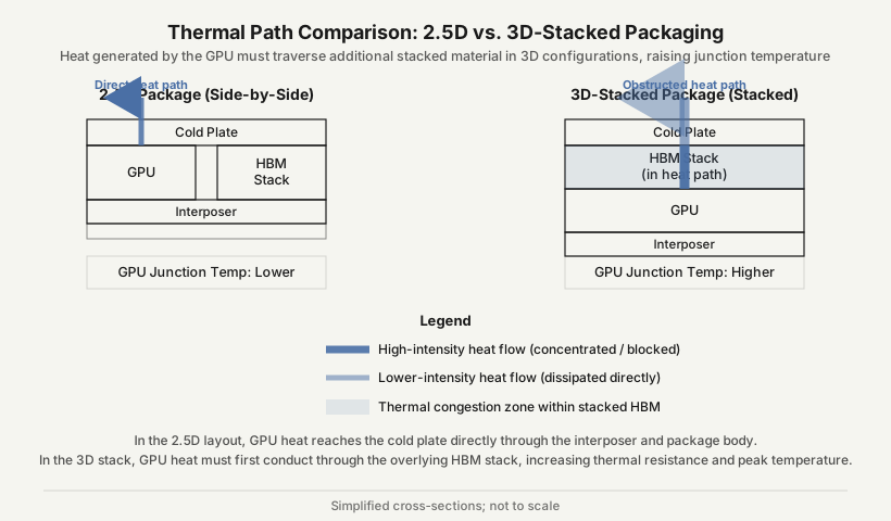
Stack the memory on top of the processor and that path changes. The processor's heat now has to travel up through the memory dies before it reaches the cooler. The memory adds heat of its own along the way. And the hottest part of the stack is at the bottom, farthest from the cooling.
imec quantified what that means in a study presented at the IEEE International Electron Devices Meeting in December 2025 — the first thermal system-technology co-optimization study of 3D HBM-on-GPU. The model placed four HBM stacks, each of twelve hybrid-bonded DRAM dies, directly on a GPU through microbumps, with cooling applied on top of the memory. Under power maps derived from AI training workloads, with the GPU modeled at 414 W and the HBM adding about 40 W:
- 2.5D baseline: peak GPU temperature of 69.1 °C
- 3D stack, no mitigation: 141.7 °C
Stacking roughly doubled the operating temperature, leaving the GPU unusable.
imec then worked the number back down, one step at a time:
- Removing the HBM base die cut about 4 °C.
- Merging the HBM stacks and thinning the top die cut more.
- Halving GPU frequency cut more than 20 °C, at a 28% workload penalty.
- Optimizing thermal silicon cut more.
- Adding double-sided cooling removed the final ~17 °C.
The end result was 70.8 °C — roughly parity with 2.5D. According to imec's James Myers, the mitigated 3D package still outperforms the 2.5D baseline despite the frequency penalty, because its smaller footprint and higher bandwidth give it higher throughput density.
That's a win, but it's also a measure of the problem. Reaching parity took six separate interventions, including throwing away 28% of the workload and adding a second cooling surface. In-silicon cooling aims to remove heat where it's generated rather than routing it through several layers first.
A Forty-Year-Old Idea
1981: channels etched into the chip
In 1981, David Tuckerman and R. F. W. Pease published a compact, water-cooled heat sink etched directly into silicon in IEEE Electron Device Letters. At a power density of 790 W/cm², they measured a maximum substrate temperature rise of 71 °C above the inlet water temperature, in close agreement with theory.
The paper also explained why channels should be small. For laminar flow in confined channels, the convective heat-transfer coefficient scales inversely with channel width — narrower channels move heat better — and coolant viscosity sets how narrow they can practically get. Every later design in this article works within that trade-off.
2008: water between the layers of a 3D stack
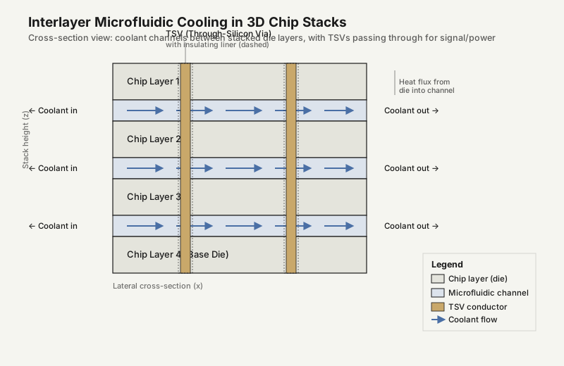
In 2008, IBM's Zurich Research Laboratory and Germany's Fraunhofer Institute tackled stacked chips specifically. Thomas Brunschwiler's team piped water through cooling structures about 50 µm wide — roughly the width of a human hair — between the individual layers of a 3D stack.
- Cooling performance: 180 W/cm² per layer, on a stack with a 4 cm² footprint
- Total heat: about 1 kW for the full stack
- Geometry: cooling layers about 100 µm high, with the whole stack about 1 mm thick
- Interconnect density: 10,000 vertical interconnects per cm²
The interconnects were the tricky part. Each through-silicon via (TSV) had to pass through a layer full of water. IBM left a silicon wall around each via and added a thin layer of silicon oxide to insulate it electrically from the coolant.
IBM's Bruno Michel explained why the effort was needed: conventional coolers mounted on the back of a chip don't scale to stacks. Interlayer cooling shortens the heat path, and its capacity grows with the number of layers — which makes stacking several high-power logic layers possible in a way backside cooling doesn't. The work won a Best Paper award at IEEE ITherm.
2012: DARPA sets the targets
DARPA's Intrachip/Interchip Enhanced Cooling (ICECool) program, with its first solicitation in June 2012, framed the approach as "embedded" thermal management. The idea was to bring microfluidic cooling inside the substrate, chip, or package, and to make thermal management part of the earliest stages of electronics design rather than something added afterward. Proposals were to flow dielectric liquids through microchannels, micropores, and inter-chip microgaps.
ICECool Fundamentals set explicit targets:
- More than 1 kW/cm² chip-level heat flux
- More than 1 kW/cm³ heat density
- 5 kW/cm² removed from sub-millimeter hot spots
In Phase I, Lockheed Martin's embedded microfluidic approach cut thermal resistance by a factor of four while cooling a demonstration die at 1 kW/cm², with multiple local hot spots at 30 kW/cm². The program has since concluded.
Co-Design: Cooling Designed With the Circuit
The most important result for efficiency came in 2020, from van Erp, Soleimanzadeh, Nela, Kampitsis, and Matioli at EPFL's Power and Wide-band-gap Electronics Research Laboratory, published in Nature.
Their approach was monolithic: microfluidic channels were designed together with the electronic devices in the same semiconductor substrate, using a manifold structure to distribute coolant, instead of being bolted onto a finished chip. The numbers:
- Heat extraction: more than 1.7 kW/cm²
- Pumping power: 0.57 W/cm²
- Coefficient of performance: above 10,000 for single-phase water cooling, a 50-fold improvement over conventional microchannels
Coefficient of performance here is heat removed divided by the power spent pumping coolant. A figure above 10,000 means the cooling system consumes a tiny fraction of the heat it carries away. The team pointed to more compact integrated power converters, and less energy spent on cooling, as direct applications.
The lesson that carries over to processors is in the method more than the device. The gain came from co-designing the channels and the electronics, rather than treating cooling and circuitry as separate problems. That's the same shift ICECool asked for: thermal design at the start of the design flow.
From Lab to Foundry: TSMC's Direct-to-Silicon Cooling
At the 2025 IEEE Electronic Components and Technology Conference (ECTC), TSMC presented "Direct-to-Silicon Liquid Cooling Integrated on CoWoS Platform." CoWoS is TSMC's advanced packaging platform for multi-die chips, so this is in-silicon cooling arriving inside a production packaging flow.
The design, called a Si-Integrated Micro Cooler (IMC-Si), is a silicon layer with etched microfluidic structures that's fusion-bonded directly to the back of the chip. That removes the thermal interface material, the paste or pad layer that normally sits between a die and its cooler and adds thermal resistance. Fusion bonding also forms a hermetic seal that holds up under high coolant pressure.
TSMC compared three channel structures — square pillars, trenches, and flat planes — and found pillars extracted heat best.
The measured results, on a 3.3×-reticle CoWoS-R package of about 3,300 mm² carrying multiple logic dies and HBM stacks:
- Junction-to-ambient thermal resistance: as low as 0.055 °C/W at a coolant flow rate of 40 ml/s
- Lidded liquid cooling with thermal interface material: 0.064 °C/W, making IMC-Si about 15% better
- Sustained power: more than 2.6 kW
- Coolant: deionized water
The process runs at low temperature, and no electrical degradation was reported. Commercialization is expected around 2027.
A 15% improvement in thermal resistance sounds incremental. But it's measured on a multi-die, multi-kilowatt package, from a foundry, with a production timeline. The earlier results in this history were research demonstrations.
Etched Into the GPU: Microsoft and Corintis
In September 2025, Microsoft described a prototype that etches channels straight into the back of a GPU. The channels are about the width of a human hair, and their layout was designed with AI by the Swiss startup Corintis. The result is a branching pattern that Microsoft compares to the veins of a leaf or a butterfly wing, routing coolant toward the chip's actual hot spots.
In tests on a server running core services for a simulated Microsoft Teams meeting:
- Heat removal was up to 3× better than cold plates
- The maximum temperature rise of the silicon inside the GPU fell by 65%
Microsoft ran four design iterations in a single year and was candid about what's still hard:
- Channel depth: deep enough to circulate enough coolant without clogging, but not so deep that the silicon weakens
- Packaging: a leak-proof package for the chip
- Chemistry and process: the right coolant formula and the right etching method
Microsoft gave no timeline for deploying the technology at scale. But the company stated the stakes plainly: "in as soon as five years, if you're still relying heavily on traditional cold plate technology, you're stuck." Corintis came out of stealth with a $24 million Series A.
Microsoft's Ricardo Bianchini also sketched where this goes for stacked chips. Liquid could flow through a 3D chip, around "cylindrical pins between the stacked chips, a bit like pillars in a multilevel parking garage." That's close to IBM's 2008 interlayer geometry, and to the pillar structures TSMC found performed best.
The Frontier: Channels Through the Whole Stack
Backside cooling, whether TSMC's or Microsoft's, reaches the top of a stack. Heat from the bottom layer still has to cross everything above it, which is the problem imec's model exposed.
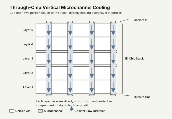
A 2023 simulation study by Lihong Ao and Aymeric Ramiere, later published in Thermal Science and Engineering Progress, takes interlayer cooling to its limit. It proposes through-chip microchannels — vertical water channels that cross the entire chip perpendicular to its layers, cooling every layer directly.
In computational fluid dynamics simulations, the best geometry was a 10 µm pitch with a 1 µm channel radius. That configuration supported more than 10⁴ W/cm² while keeping the maximum temperature rise below 60 K with 300 K inlet water. The key property is that cooling performance doesn't depend on the number of layers for a given chip thickness. Add layers and the cooling doesn't degrade.
The authors acknowledge the manufacturing challenges. This is a simulation, not a fabricated device, and its direction matters more than its headline number.
What Still Stands in the Way
Across forty years of results, the same obstacles come up:
- Mechanical integrity. Every channel removes silicon. Microsoft names the depth trade-off directly: enough flow, without weakening the die.
- Sealing. Coolant at the die means a leak happens at the die itself. TSMC's answer is hermetic fusion bonding, and IBM's is oxide-lined walls around every via.
- Clogging and coolant chemistry. Channels the width of a hair can block. Microsoft lists coolant formulation as an open problem.
- Buried layers. Backside approaches don't reach the bottom of a stack. Interlayer and through-chip channels do, but they collide with the dense vertical interconnects that make stacking worthwhile.
- Design flow. EPFL's efficiency came from designing channels with the circuit. That means thermal-fluidic layout becomes part of chip design, which is a tooling and process change for the whole industry, not just a new cooler.
Where This Goes Next
Speculation: Cooling is moving from a rack and heat-sink decision toward a packaging and die-design decision. When the cooler is fusion-bonded to the die at the foundry, as in TSMC's approach, the thermal interface is set before the part reaches a server builder.
Speculation: The die backside is becoming contested. Our coverage of "Backside Power Delivery Networks and the Path to 2nm Yield Recovery" described moving power delivery to the back of the wafer, and backside microchannels want the same surface. How the two will share it is an open engineering question, and one that is likely to shape how far either technology goes on leading-edge logic.
Speculation: For memory-on-logic stacks, the steps imec used — thinning, merging stacks, frequency limits, double-sided cooling — look like a bridge. The approaches that scale with layer count are the ones that put fluid between or through the layers, as IBM demonstrated in 2008 and Ao and Ramiere modeled in 2023. Whether they reach production depends on solving the via-sealing and manufacturing problems, not on the basic heat-transfer scaling, which Tuckerman and Pease laid out in 1981.
This article follows our "Liquid Cooling Architectures for Exascale Data Centers" from the rack down into the die, and connects to "Chiplets and the UCIe Standard" and "Backside Power Delivery Networks and the Path to 2nm Yield Recovery." Next in this thread: the memory side of the stack — 3D-stacked SRAM and cache-on-logic, where the bandwidth gains that motivate stacking run straight into the thermal limits described here.