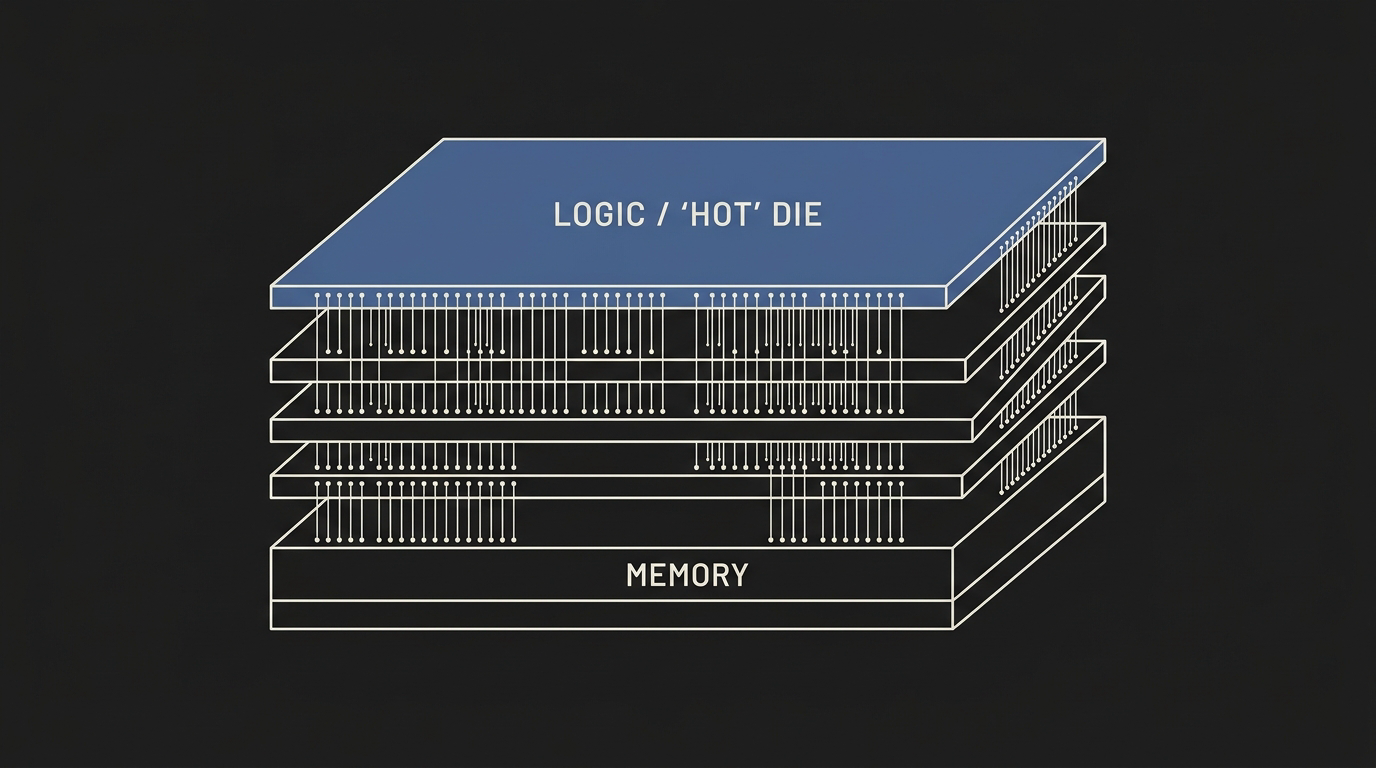
Memory Goes Underneath: 3D-Stacked Cache, Cache-on-Logic, and the Thermal Price of Bandwidth
At a Glance
- Why stack memory at all: LLM decoding is limited by memory bandwidth more than compute. Stacking memory directly on logic replaces package-length wires with vertical bonds — AMD's hybrid-bonded 3D chiplets offer more than 200× the interconnect density of 2D chiplets, and d-Matrix reports about 20× the bandwidth per square millimeter of HBM.
- The first design put memory on top: AMD's 2021 3D V-Cache bonded 64 MB of SRAM on top of a Ryzen core complex die. It worked, and it also sat between the hottest silicon and the cooler. The Ryzen 7 5800X3D shipped with a 1.35 V limit instead of the 5800X's 1.5 V.
- The second design flipped it: In the 2024 Ryzen 7 9800X3D, AMD moved the cache below the cores so the compute die touches the cooling path. It became the first fully unlocked X3D chip, with the highest clock speeds of the line.
- The data center is making the same move: d-Matrix's Raptor, detailed at Hot Chips 2026, puts a TSMC N4 logic die on top of 3D DRAM, keeps the DRAM under 100 °C with liquid cooling, and caps logic power density at 0.5 W/mm².
- When memory has to stay on top, schedule around the heat: The Tasa research architecture keeps DRAM stacked over logic and uses heterogeneous cores to cut peak temperature by up to 9.37 °C, while still reporting a 2.85× Llama-65B speedup over GPU baselines.
In "CXL 3.0 and the End of the Memory Wall," we looked at memory bandwidth and capacity across a rack. This is the same constraint at the other end of the scale — a few microns instead of a few meters. It also picks up directly from "Cooling From Inside the Silicon," where imec's model showed high-bandwidth memory stacked on a GPU pushing it to 141.7 °C. That piece asked how to pull heat out of a stack. This one looks at a simpler lever that's already shipping: which way up the stack goes.
Why Stack Memory on Logic
Generating a token in a large language model means reading model weights and the growing key-value cache out of memory, again and again. In their 2025 paper on the Tasa architecture, Siyuan He, Peiran Yan, Yandong He, Youwei Zhuo, and Tianyu Jia put it directly: autoregressive decoding is the major inference bottleneck because its operations are memory-intensive and hardware bandwidth is limited.
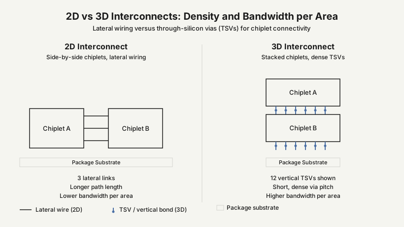
Bandwidth is set by the wires between memory and compute — how many there are, how long, and how much energy each bit takes to push across. Stacking attacks all three.
Interconnect density. When AMD introduced its 3D chiplet technology at Computex 2021, it described a hybrid bond with through-silicon vias (TSVs). A direct copper-to-copper bond with no microbumps gave more than 200 times the interconnect density of 2D chiplets, more than 15 times the density of microbump-based 3D stacking, and three times better interconnect energy efficiency. AMD also said the bumpless interface improved thermals and interconnect pitch.
Bandwidth per area. At Hot Chips 2026, d-Matrix reported about 32.6 GB/s per square millimeter for its stacked 3D DRAM, against roughly 1.5 GB/s for HBM — around 20 times.
Energy per bit. d-Matrix put its 3D DRAM I/O energy at about 0.3–0.4 pJ, against 2.5–5 pJ for HBM4. Measured as power per unit of bandwidth, that's 2.96 mW per GB/s versus 40 mW, a 13.5× improvement.
Those d-Matrix figures come from the vendor's own presentation. But the direction matches what AMD reported in 2021: vertical bonds are denser and more energy-efficient per bit than lateral ones.
The cost is heat. Stacking puts one die in the other's thermal path, and which die ends up in the way turns out to matter a great deal.
Generation One: Cache on Top
AMD's first application of its 3D chiplet technology was 3D V-Cache: 64 MB of 7 nm SRAM bonded vertically on top of the Ryzen 5000 core complex die (CCD), tripling the L3 cache. At Computex 2021, a modified Ryzen 9 5900X prototype showed an average gain of about 15% in 1080p gaming.
The product that shipped, the Ryzen 7 5800X3D, stacked the 64 MB chiplet over the CCD's own 32 MB of L3 for 96 MB total, using TSMC's SoIC bonding.
The thermal side showed up in the specifications. AMD said the cache chiplet and the CCD share a power plane, and set an effective voltage limit of 1.35 V — below the 1.5 V limit of the standard Ryzen 7 5800X. Tom's Hardware noted that the extra SRAM die and the silicon shim beside it reduce heat dissipation from the bottom die, leaving less thermal headroom, and suggested the voltage limit may be a product decision to keep temperatures in check rather than a hard physical limit.
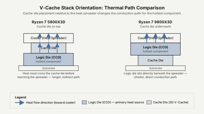
The mechanism is straightforward. The cores generate most of the heat, and the cooler sits on top of the package. With the cache layer over the CCD, heat from the cores had to pass through it before reaching the heat spreader — and the cache added heat of its own. The CPU had to be configured to run cooler to compensate.
Generation Two: Cache Underneath
For the Ryzen 7 9800X3D, launched October 31, 2024, AMD kept 64 MB of stacked cache but turned the stack over. AMD said it moved the cache memory below the processor, placing the core complex die closer to the cooling solution to help keep the Zen 5 cores cooler.
The results, per AMD:
- Clock speeds: 4.7 GHz base and 5.2 GHz maximum boost — the highest of any X3D chip
- Overclocking: the first X3D processor to be fully unlocked
- Gaming performance: up to an average 8% improvement over the previous generation
- Configuration: 120 W TDP and 104 MB total cache
This is the central lesson. Putting memory on top of logic produced a manufacturable, shipping product. But it constrained the part of the chip that makes the most heat. Putting memory underneath let the hot die touch the cooling path directly, and the constraints on voltage, clock speed, and overclocking relaxed.
The flip moves the compromise rather than eliminating it. As Tom's Hardware put it in its review, the cache likely can't be clocked quite as high in its new position, but the cores are better cooled and don't need to be held back as much.
The Data Center Version: Logic on Top of 3D DRAM
d-Matrix announced a collaboration with ASIC design firm Alchip in November 2025 around 3DIMC, its 3D-stacked DRAM in-memory compute technology. The technology had been validated on Pavehawk test silicon in d-Matrix's labs, and Raptor — the successor to d-Matrix's Corsair accelerator — was named as the commercial product. The company claimed up to 10× faster inference than HBM4-based solutions and gave no launch date.

At Hot Chips 2026, d-Matrix showed how Raptor is built, and its orientation matches the 9800X3D's:
- Stack: a TSMC N4 logic die sits on top of a 3D DRAM die
- Bonding: 36 µm face-to-face stacking, which d-Matrix describes as proven, low-cost, high-volume, and high-yield
- Capacity: 32 GB per card in a single-high configuration
- Thermal envelope: liquid-cooled systems keep the DRAM under 100 °C, with logic power density held to no more than 0.5 W/mm²
That last constraint shows what the logic-on-top orientation still costs. Even with the hot die facing the coolant, the DRAM beneath it has a temperature ceiling. The logic's power density is capped to protect memory that can't be cooled directly.
d-Matrix also claims about 1,000 tokens per second per user when serving a 3-trillion-parameter-class model at 1 million tokens of context, and says a 72-card scale-up can host a frontier model at that context length. Those are vendor claims about a product that isn't independently benchmarked yet, and they should be read that way. The architecture choices — logic up, memory down, liquid cooling, an explicit power-density cap — are the part that's already concrete.
When Memory Stays on Top: Thermal-Aware Architecture
Not every design can flip. Many 3D-stacked proposals keep multiple DRAM dies over the logic die, and so did imec's HBM-on-GPU model, which reached 141.7 °C without mitigation against 69.1 °C for a side-by-side 2.5D layout.
The Tasa paper starts from that configuration and measures the problem. Its authors report that stacking DRAM on logic produces more severe thermal issues than a 2D architecture on three counts: peak temperature, temperature gradient across the die, and how temperature scales as more cores are added.
Their answer works at the architecture and scheduling level instead of changing the stack:
- Heterogeneous cores. High-performance cores handle compute-intensive operations, and high-efficiency cores handle memory-intensive operators such as attention layers.
- Cross-stack thermal optimization. The layout balances temperature across the stack rather than letting hot spots stay under the memory.
- Bandwidth-sharing scheduling. Memory bandwidth is shared across the heterogeneous cores to keep it fully used.
Compared with a homogeneous 3D-stacked design, Tasa cut peak temperature by up to 5.55 °C with 48 cores, 9.37 °C with 60, and 7.91 °C with 72. On performance, it reported a 2.85× speedup for Llama-65B inference over GPU baselines, and a 2.21× speedup for GPT-3 66B over a state-of-the-art heterogeneous processing-in-memory LLM accelerator.
The useful point is that the two goals aren't simply opposed. Matching core type to operator type spreads heat more evenly and uses bandwidth better. A design that ignores the thermal map tends to lose on both.
imec reached a related conclusion at package scale: even after halving GPU frequency — a 28% workload penalty — its mitigated 3D stack outperformed the 2.5D baseline because of higher throughput density. Stacking still wins when the heat is managed. The question is how much performance the management costs.
What the Pattern Says
Across a consumer CPU, a data center inference accelerator, a research architecture, and a thermal study, the same rule comes through:
- Put the hottest die against the cooling path. AMD moved from cache-on-top (2021–2022) to cache-underneath (2024), and d-Matrix built Raptor logic-on-top.
- Budget power density for the die that can't be cooled. d-Matrix's 0.5 W/mm² cap exists to keep buried DRAM under 100 °C.
- If memory must stay on top, make the architecture thermal-aware. Tasa's heterogeneous cores and imec's co-optimization steps recover much of what stacking costs.
- Treat vendor multipliers as claims. d-Matrix's 10× and 1,000 tokens/s figures aren't independently measured yet. AMD's orientation change, by contrast, is visible in shipping specifications.
Speculation: Logic-on-memory looks likely to become the default orientation for high-power AI logic with stacked memory, because it puts the dominant heat source next to the coolant. The cost moves to the power-delivery and signal paths through the memory die, and to power-density limits set by the memory's temperature tolerance. That links this topic to backside power delivery and to in-silicon cooling. Both change what the bottom of a stack can carry and how much heat it can shed.
Speculation: Tasa's approach — assigning operators to cores according to their thermal and bandwidth cost — could move up into compilers and serving runtimes, which would place work based on where a stacked memory hierarchy is running hot at a given moment. None of the sources here demonstrate that above the architecture level.
This article continues our memory-wall coverage from "CXL 3.0 and the End of the Memory Wall" down to the package, and builds on "Cooling From Inside the Silicon" and "Chiplets and the UCIe Standard." Future pieces in this thread will look at thermal-aware scheduling in compilers and serving runtimes, and at the economics of hybrid bonding as it moves from consumer CPUs into AI accelerators.