Wafer-Scale Chips and the Yield Problem: Two Ways to Build a Computer That Can't Be Defect-Free
At a Glance
- The obstacle: No wafer comes out of a fab defect-free. A chip the size of a whole wafer will always contain flaws, which is why Gene Amdahl's Trilogy Systems, founded in 1980 to build fault-tolerant wafer-scale chips, found its designs feasible but too expensive to produce.
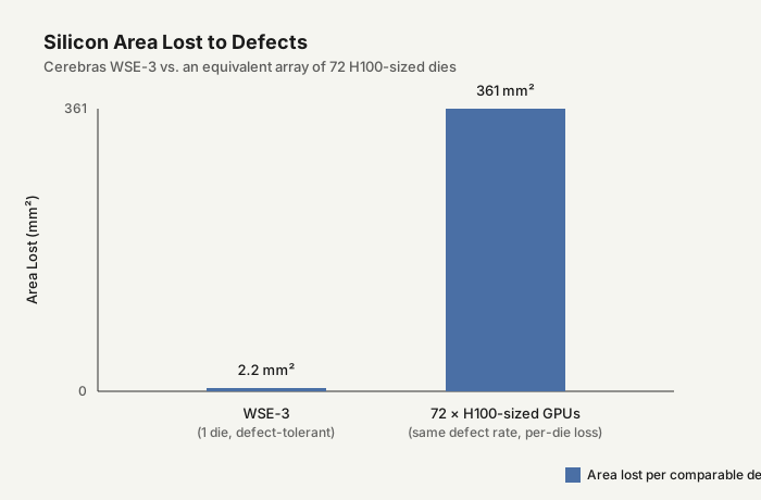
- Approach one — build it whole and route around defects: Cerebras makes a single 46,225 mm² chip with 970,000 physical cores and ships 900,000 of them active. Its cores are so small (about 0.05 mm²) that, by Cerebras' estimate, a wafer's worth of defects costs 2.2 mm² of silicon, against 361 mm² for the same defect rate across 72 GPU-sized dies.
- Approach two — test pieces first, then assemble a wafer: A UCLA–Illinois prototype bonded 2,048 pre-tested chiplets onto a wafer-scale silicon substrate. Doubling the Fundamentals of Semiconductor Manufacturing raised per-chiplet bonding yield from 81.46% to 99.998%, and a second independent network cut disconnected paths from over 12% to under 2% when five chiplets failed.
- The foundry has chosen a direction: TSMC's SoW-X, a CoWoS-based wafer-sized system claimed at 40 times the computing power of current CoWoS, is scheduled for volume production in 2027.
- Yield isn't the only risk: Tesla built Dojo from 25 chips per wafer-sized tile, then shut the program down in 2025, calling its next version "an evolutionary dead end."
"Chiplets and the UCIe Standard" looked at how processors are being split into smaller dies joined in a package. Wafer-scale integration takes the opposite extreme — a system the size of a whole silicon wafer — and runs straight into the problem chiplets exist to avoid. Large silicon collects defects. This article is about the two engineering strategies for living with that fact.
Why Nobody Builds Wafer-Sized Chips (Until Recently)
Chips are normally limited by the reticle: the area a lithography scanner can expose in one shot. A wafer is printed as a grid of identical dies, separated by scribe lines — narrow lanes used for sawing the wafer apart and for test structures. Each die is designed to be independent, and defective ones are thrown away.
That throwaway is the yield model the industry relies on. A random defect kills whichever die it lands on, and a die's odds of surviving fall as its area grows. Make one die the size of the whole wafer and, under that model, nothing survives.
Trilogy Systems ran into this in the 1980s. Gene Amdahl founded the company in 1980 to build fault-tolerant wafer-scale chips that would combine the functions of a hundred different chips into one. According to the Engineering and Technology History Wiki, the designs "proved feasible but excessively expensive to produce." Weather damage to the company's chip plant added to the trouble. Trilogy spent much of its capital and ended up buying a computer maker, Elxsi, to survive.
The modern answer, as Cerebras describes it, is an architecture designed to expect defects rather than be killed by them.
Approach One: One Wafer, Many Spares
How Cerebras connects the dies
At Hot Chips in 2019, Cerebras' Sean Lie presented the first Wafer Scale Engine: 46,225 mm² of silicon, 1.2 trillion transistors, 400,000 cores, and 18 GB of on-chip memory on TSMC's 16 nm process. The talk listed five problems that had to be solved: cross-die connectivity, yield, thermal expansion, package assembly, and power and cooling.
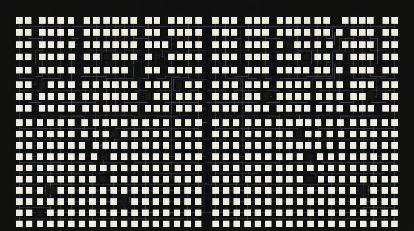
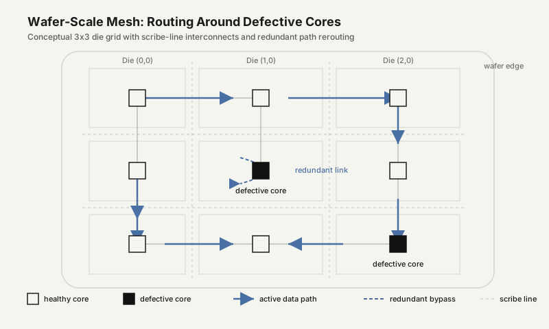
The first is solved in the scribe lines. The wafer is still printed as a grid of ordinary dies, but Cerebras and TSMC added wires across the scribe lines, extending each die's 2D mesh network into its neighbors. The result is a single homogeneous array of cores in which crossing a die boundary looks the same as any other hop.
How it handles defects
Cerebras' 2019 slides stated the premise directly: it is "Semiconductor Manufacturing Technology." The answer was redundancy built into the architecture:
- A uniform, small core design makes redundancy cheap.
- Redundant cores replace defective ones.
- Redundant fabric links reconnect the network so the software still sees a logical 2D mesh.
In January 2025, Cerebras' James Wang put numbers to the approach for the third-generation WSE-3, which has 4 trillion transistors on TSMC's 5 nm process and 44 GB of on-chip SRAM:
- Each WSE-3 core is about 0.05 mm², roughly 1% of the ~6 mm² streaming-multiprocessor core in an Nvidia H100.
- Assuming about 0.001 defects per mm² for TSMC's 5 nm process, a WSE-3 would see about 46 defects. If each disables one core, the silicon lost is about 2.2 mm².
- The same defect density across 72 H100-sized GPUs (58,608 mm²) gives about 59 defects. Because each defect disables a much larger core, that's about 361 mm² of lost silicon — 164 times more.
- The WSE-3 has 970,000 physical cores and ships with 900,000 active, so 93% of cores are in use.
This is Cerebras' own first-order model rather than measured fab data, and a defect can do more than disable one core. But the logic is sound. Yield loss scales with the size of the unit a defect destroys. Make that unit tiny and uniform, keep spares, and the network can route around the damage.
What else changes at wafer size
Yield isn't the only thing that breaks. The 2019 talk described three physical problems a normal package never has:
- Thermal expansion. Silicon and circuit boards expand at different rates, and across a wafer that difference produces too much mechanical stress for conventional packaging. Cerebras built a custom connector that absorbs the variation while keeping electrical contact.
- Assembly. No standard package exists for a wafer-sized chip, so Cerebras developed custom machines and processes to align the board, connector, wafer, and cold plate.
- Power and cooling. Current density is too high to distribute through board power planes, and heat density is too high for air. Power enters perpendicular to the wafer, and water carries heat away through a cold plate.
Approach Two: Test First, Then Assemble
The alternative is to never put untested silicon onto the wafer.
The 2,048-chiplet prototype
At the 2021 Design Automation Conference, a UCLA and University of Illinois team — Pal, Gupta, Kumar, Iyer and colleagues — described a waferscale processor built from 2,048 chiplets. They framed the choice directly. Monolithic wafer-scale chips are homogeneous, so they can't include dense memory made on a different process, and they need redundant cores and links reserved for yield. Their alternative was to bond pre-tested, known-good bare dies onto a wafer-scale interconnect substrate.
The substrate was Silicon Interconnect Fabric (Si-IF), a passive silicon wafer carrying only wiring:
- Copper-pillar connections at a 10 µm pitch, at least 16 times denser than the microbumps used on interposers
- About 100 µm between chiplets
- 5 µm wiring pitch on two signal layers, giving 400 wires per millimeter of chiplet edge
The system was 1,024 tiles of two chiplets each, about 15,000 mm² in all, built on TSMC's 40 nm low-power process:
- A compute chiplet with 14 ARM Cortex-M3 cores, each with 64 KB of SRAM, plus network routers and power-regulation circuits
- A memory chiplet with five 128 KB SRAM banks
With so many unknowns in the manufacturing process, fault tolerance drove the design.
Yield moves to the bonds
Testing chiplets before assembly removes fabrication defects from the equation, but it creates a new yield problem: millions of tiny bonds. The system has more than 3.7 million inter-chip connections.
A single copper pillar bonds successfully more than 99.99% of the time. That sounds safe until you multiply. With more than 2,000 connections per chiplet, only 81.46% of chiplets would bond perfectly, leaving an expected 380 faulty chiplets on the wafer.
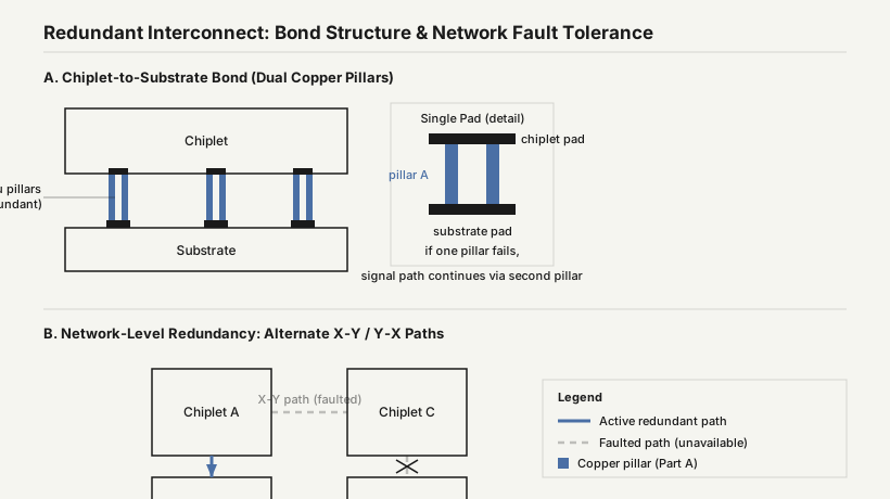
The team's fix was physical redundancy. Each I/O pad was sized to take two copper pillars, so a connection fails only if both do. That raised per-chiplet bonding yield to 99.998% and cut the expected faulty chiplets from 380 to about 1. The I/O cells stayed small (0.4 mm² per chiplet in total) and efficient (0.063 pJ per bit), helped by the fact that bare-die bonding needs to survive only 100 V electrostatic discharge rather than the 2 kV required of packaged parts.
Yield moves to the network
Even one or two dead chiplets can break communication. The team modeled a standard mesh with deterministic dimension-ordered routing. With just five faulty chiplets out of 2,048, more than 12% of source–destination paths were disconnected.
The fix was a second network. The wafer carries two independent meshes: one routes X-then-Y, the other Y-then-X. Most chiplet pairs now have two distinct paths, and with five faulty chiplets, disconnected paths fell to under 2%. Requests and responses travel on complementary networks, so two-way communication works as long as either path survives. After assembly, the system records faulty tiles in a fault map, and kernel software chooses which network each pair uses. For the few pairs still cut off, software can relay traffic through an intermediate tile.
The same thinking extends to the clock. A fast clock forwarded from the wafer edge reaches every working tile unless all four of a tile's neighbors are faulty.
Power delivery and testing
Delivering power across the wafer was its own challenge. Feeding the chiplets at logic voltage would mean about 290 A at 1.21 V and large voltage droop across the substrate. The team instead delivered 2.5 V at the wafer edge and regulated it on each chiplet. Chiplets far from the edge see supply as low as 1.4 V, which their regulators bring to 1.0–1.2 V.
Testing was built in at both ends. Each chiplet carries larger duplicate pads for probe-card testing before bonding, while only the untouched fine-pitch pads are bonded. After assembly, a progressive JTAG scheme locates faulty chiplets across the wafer.
Industrial Versions of the Chiplet Route
Tesla Dojo used a related approach at production scale. Its training tile placed a 5×5 array of D1 processors, each about 50 billion transistors on TSMC's 7 nm process, onto a carrier wafer using TSMC's integrated fan-out system-on-wafer (InFO-SoW) packaging.
Then, in August 2025, Tesla disbanded the Dojo team. Elon Musk said that "all paths converged to AI6" and that "Dojo 2 was now an evolutionary dead end," shifting resources to Tesla's AI5 and AI6 inference chips. Nothing in that explanation points to yield or packaging failure. It's a reminder that a wafer-scale system also has to fit a company's software and chip roadmap, and that the hardware working isn't enough.
TSMC SoW-X is the foundry's version of the same idea. At its April 2025 technology symposium, TSMC described SoW-X as "a CoWoS-based offering to create a wafer-sized system with computing power 40X the current CoWoS solution," with volume production scheduled for 2027. Alongside it, TSMC announced 9.5-reticle CoWoS for 2027, able to hold 12 or more HBM stacks, and integrated voltage regulators with five times the vertical power density of a separate power management chip.
Comparing the Two Philosophies
| Monolithic with spares (Cerebras) | Known-good chiplets on a wafer (UCLA/UIUC, Dojo, SoW-X) | |
|---|---|---|
| Where defects are handled | After fabrication, by disabling cores and rerouting | Before assembly, by testing and discarding bad dies |
| New yield risk | Defects must stay small and random | Millions of bonds and assembly steps |
| Redundancy lives in | Spare cores and fabric links | Redundant bond pillars, dual networks, fault maps |
| Heterogeneity | One process, one die type | Compute and memory from different processes possible |
| Shared physical problems | Thermal expansion, power delivery, cooling | Same |
Both approaches reach the same principle from different directions: redundancy is cheapest when the repeated unit is small. Cerebras makes the core small so a defect costs 0.05 mm². The UCLA team makes the bond redundant so one bad pillar costs nothing. Neither tries to prevent defects. Both design so that a defect doesn't matter.
Speculation: The chiplet-on-wafer route looks likely to dominate commercial wafer-scale systems. With SoW-X on a 2027 schedule, it becomes a foundry product rather than a custom program. Its heterogeneity advantage also lines up with where AI systems are going — memory bandwidth, not just logic. Monolithic wafer-scale keeps the advantage of uniform on-wafer wiring with no bond interfaces, and Cerebras shows that model can ship.
Speculation: Whichever route wins, the constraints that remain are the physical ones both share. A wafer-sized system has to get power in vertically and heat out at densities no normal package handles, which ties this topic to in-silicon cooling ("Cooling From Inside the Silicon") and to high-density power conversion ("Solid-State Transformers").
This article extends our chiplet coverage from "Chiplets and the UCIe Standard" to the wafer scale, and connects to "Cooling From Inside the Silicon" and "Memory Goes Underneath." A natural follow-up is the power side: delivering hundreds of amps vertically into a wafer-sized system, and what integrated voltage regulators change.
Stay in the loop. Project Isocline publishes deep-dive technical analysis on AI infrastructure, energy systems, and the engineering decisions shaping the next decade of compute. No noise. No fluff.
You can unsubscribe at any time.